Features
- Input range: 2.7V to 42V, supporting cold crank
- Integrated power management:
- Buck-Boost DC/DC1 5.7V
- Buck DC/DC2 resistor programmable
- Five linear regulators (LDOs), with configurable options for tracking and protection
- Low IQ modes:
- Power-off standby mode: 16μA
- DeepSTOP mode: 160μA
- EOT (Engine Off Timer) mode: 25μA
- Switching frequency: Selectable or fixed options with spread spectrum clocking
- Robust design:
- High-current FET drivers
- Watchdog options (QA or SPI-based)
- MCU error handling and reset features
- AEC-Q100 qualified (Grade 1)


Description
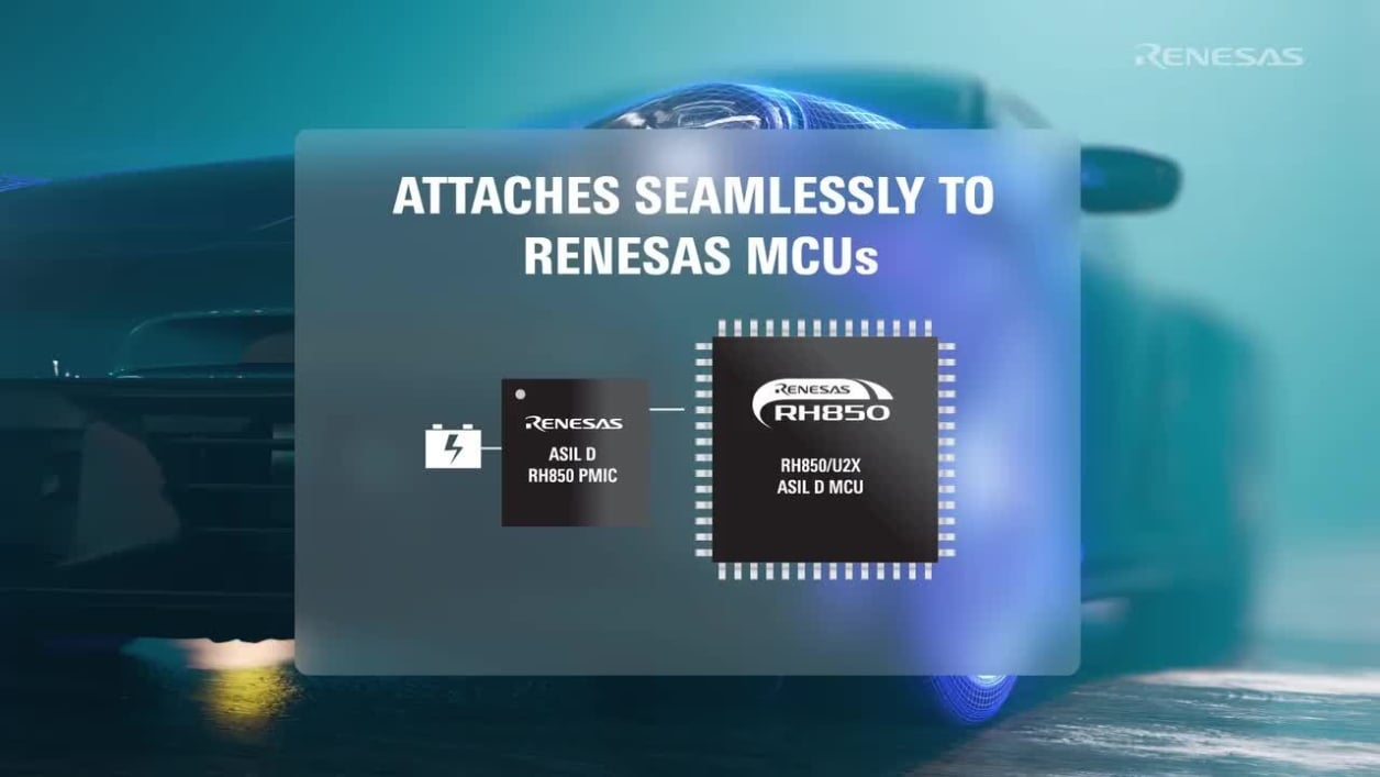
The RAA271084 Automotive Safety Integrity Level D (ASIL D) and RAA271084-B (ASIL B) are general-purpose Power Management Integrated Circuits (PMICs) with a high-voltage front-end, optimized for MCU power in automotive applications. They feature a high-voltage buck/boost controller, a low-voltage synchronous buck controller, and five linear regulators (LDOs), two of which can operate as trackers.
The RAA271084 supports ASIL D system safety goals, while the RAA271084-B supports ASIL B. Both include key safety features such as voltage monitoring, temperature monitors, watchdog timer, reset generator, and a safety-control state machine.
Available in 48-lead SCQFN and LQFP-EP packages (RAA271084) and SCQFN (RAA271084-B), both devices are AEC-Q100 Grade 1 qualified for -40°C to 125°C operation. These products are intended for ISO 26262-compliant applications, though safety analysis and assessment are ongoing and subject to change.
Parameters
| Attributes | Value |
|---|---|
| Qualification Level | Automotive |
| Product Type | MCU |
| Processor Supplier | Renesas |
| Processor Name | RH850 C1x, E1x, F1x, P1x, E2x, U2A, U2B, U2C |
| Total step-down DC/DC converter channels (#) | 2 |
| Step-up DC/DC converter Channels (#) | 1 |
| Input Voltage (Min) (V) | 2.7 |
| Input Voltage (Max) (V) | 42 |
| Bus Voltage (Max) (V) | 5.5 |
| Output Current Max (A) | 10 |
| Outputs (#) | 7 |
| Function | 7-ch ASIL B PMIC, 7-ch ASIL D PMIC |
| Comm. Interface | SPI |
| Battery Interface | No |
| GPIOs (#) | 0 |
| Integrated Battery Charger | No |
| Switching Frequency (MHz) | 0.44 - 2.2 |
Application Block Diagrams
 | Three-Level T-Type Traction Motor Inverter Three-level T-type traction motor inverter delivering higher efficiency, reduced EMI, and smoother motor control for next-generation 800V+ EV platforms. |
 | Humanoid Battery Management System Integrated humanoid robot BMS enabling safe, real-time power management, protection, and battery-state control. |
 | Inverter Reference Platform with Optimized Pulse Pattern (OPP) Efficient xEV inverter platform with OPP control for low distortion, stable torque, and fast integration. |
 | X-in-1 Electric Vehicle Unit Integrated X-in-1 EV power system for efficient motor control, charging, and DC/DC conversion. |
Additional Applications
- Automotive power-train systems
- Automotive gateway systems
- Ideal power supply for RH850 U2x MCUs
Complete Your Design
Explore complementary products to elevate your design
Renesas Boards & Kits
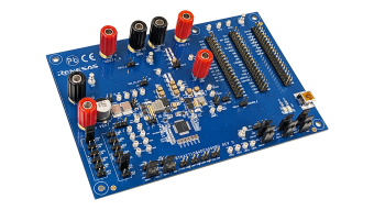
Evaluation Board for RAA271084 Scalable ASIL D Microcontroller PMIC
The RTKA271084DE0000BU evaluates the performance of the RAA271084 automotive PMIC, which features a high-voltage primary buck/boost controller, a low-voltage synchronous buck controller, and five low-dropout linear regulators (LDOs), two of which can be used as trackers. The evaluation board is... Read More

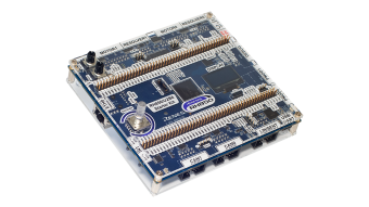
RH850/U2B10 Target Board with Power Management IC RAA271084 (ASIL D)
The RH850/U2B10 and Power Management IC Target Board serves as an evaluation board with Arduino form factor. The circuit shows a possible implementation of the RH850/U2B10 MCU and an RAA271084 power management IC.
RH850/U2B Starter Kits
The RH850/U2B Starter Kit is a compact platform for evaluating Renesas 32-bit RH850/U2B microcontrollers. Powered by four RH850G4MH2 cores at 400MHz, it delivers high-performance real-time processing for automotive applications.
The kit includes a 12V power supply with the ASIL D-compliant Read More
