Features
- Improved Pin-to-pin to FPF2280/MAX14699
- >100V-tolerant TVS (IEC 61000-4-5)
- Maximum VIN DC Rating: 29V
- High-performance nFET: 23mΩ/4.5A
- Fixed VIN Undervoltage Lockout
- Resistor-adjustable VIN Overvoltage Lockout [or fixed 6.5V default (OVLO = GND)]
- Fast OVP Response Time: 50ns
- Overcurrent Protection: 7A
- Thermal Shutdown Protection
- ON-OFF Control: Active LOW

Description
The SLG59H1313C high-voltage load switch features a low 23mΩ RDSON internal nFET and protects low‑voltage 2.5Vdc to 5.5Vdc operating systems against voltage faults up to 29Vdc. An internal clamp circuit protects the downstream components from surge voltage up to 100V. The SLG59H1313C features a fast 50ns (typ.) overvoltage response time that turns off the internal nFET if the input voltage exceeds the OVP threshold. The OVP threshold is adjustable with optional external resistors to any voltage between 4V and 20V. Over‑temperature protection powers down the device at 145 °C (typ.). SLG59H1313C also features an overcurrent protection that turns off the switch if the current exceeds 7A (typ.), this gives additional protection from overheating the device. SLG59H1313C incorporates an open-drain output PG pin. When VIN_min < VIN < VOVLO and the switch is on, PG will be driven low indicating a good power input, otherwise, it is high impedance.
Parameters
| Attributes | Value |
|---|---|
| FET Pass Device Type | Single N-Channel |
| VIN Channel 1 min. (V) | 2.5 |
| VIN Channel 1 max. (V) | 20 |
| Input Quiescent Current Channel 1, typ (µA) | 245 |
| Input Quiescent Current Channel 1, max (µA) | 310 |
| Input Quiescent Current when OFF Channel 1, typ (µA) | 0.15 |
| Input Quiescent Current when OFF Channel 1, max (µA) | 1 |
| RDSON (Typ) Channel 1 (mΩ) | 23 |
| IDS Channel 1 (A) | 4.5 |
| Enable | Active Low |
| Output Voltage Slew Rate set by | No |
| Discharge Circuit | No |
| Undervoltage Protection | No |
| Over Voltage Protection | Yes |
| Power Good (PG), FAULT indicator | PG |
| Reverse current blocking | No |
| Reverse voltage detection | No |
| Over Current Protection (OCP) | Internally Fixed |
| Over Current Protection Setting Range Channel 1 | 7 - 7 |
| Short Circuit Protection | Yes |
| Over Temperature Protection (OTP) | Yes |
| Current Monitor Output | No |
| Internal TVS Surge Protection | Yes |
| Temp. Range (°C) | -40 to +85°C |
Application Block Diagrams
 | Pet Camera Robot Mobile pet camera robot with real-time video, audio, and wireless control. |
 | Multi-Cell USB PD Power Bank with Quick Charge 2.0/3.0 60W+ USB PD power bank offers efficient charging with multi-cell setup and Bluetooth LE monitoring. |
 | High-Performance Human Machine Interface (HMI) System Versatile system on module (SoM) for driving a wide range of human machine interface capabilities. |
 | Multi-Display HMI SoM SOM with optimized power and timing supports multi-display embedded applications. |
Additional Applications
- Wearable Devices
- Tablet PCs and Smartphones
Complete Your Design
Explore complementary products to elevate your design
| Part Number | Status | Samples | Stock | Package | Budgetary Price (USD) | Lead Count (#) | Carrier Type | Moisture Sensitivity Level (MSL) | Pb (Lead) Free | Temp. Range (°C) | Country of Assembly | Country of Wafer Fabrication |
|---|---|---|---|---|---|---|---|---|---|---|---|---|
| SLG59H1313C | Active | Available | In Stock | WLCSP | 1ku | $0.283 | 12# | Tape & Reel | 1 | Yes | -40 to +85°C | TAIWAN | TAIWAN |
| SLG59H1313CTR | Active | N/A | Out of Stock | WLCSP | 12# | -40 to +85°C |
Complete Your Design
Explore complementary products to elevate your design
Filters
Applied Filters
- GuideGreenFET load switches are designed for efficient high‑side power control in low‑voltage applications. These devices combine low RDS(on), compact packaging, and integrated protection features to replace discrete designs, reducing PCB space and improving system reliability. This guide enables engineers to quickly compare key parameters and select the optimal device for their application.
- Application NotePDF 911 KB Feb 22, 2019AI-generated Summary: Extending the maximum operating current of GreenFET load switches can be achieved by using two lower-current devices in parallel, maintaining protection features and reducing overall RDSON. Parallel operation balances current sharing due to low RDSON variation in Renesas's MOSFET design. Examples include using pairs of SLG59H1006V and SLG59M1714V devices, with detailed operational waveforms and recommended PCB layouts provided. High-current single devices like SLG59M1568V are also covered. The document includes application diagrams, oscilloscope captures, and design guidelines for high-current load switch applications.
- Application NotePDF 1.07 MB Nov 11, 2018AI-generated Summary: GreenFET load switches enable efficient power-splitting designs that accommodate multiple input voltages while providing system-level protections such as over-voltage, over-current, and surge protection. Various configurations using SLG59H1313C, SLG59H1008V, SLG59H1006V, and SLG59H1302C devices demonstrate scalable solutions for switching power rails between 5 V, 12 V, and 24 V inputs. The designs include detailed schematics and timing waveforms to illustrate operation and transitions, optimizing power consumption and protection features for modern compact electronics requiring flexible power management.
Recommended Documents (1)
Datasheets (1)
- GuideGreenFET load switches are designed for efficient high‑side power control in low‑voltage applications. These devices combine low RDS(on), compact packaging, and integrated protection features to replace discrete designs, reducing PCB space and improving system reliability. This guide enables engineers to quickly compare key parameters and select the optimal device for their application.
Manuals & Guides (1)
- Application NotePDF 911 KB Feb 22, 2019AI-generated Summary: Extending the maximum operating current of GreenFET load switches can be achieved by using two lower-current devices in parallel, maintaining protection features and reducing overall RDSON. Parallel operation balances current sharing due to low RDSON variation in Renesas's MOSFET design. Examples include using pairs of SLG59H1006V and SLG59M1714V devices, with detailed operational waveforms and recommended PCB layouts provided. High-current single devices like SLG59M1568V are also covered. The document includes application diagrams, oscilloscope captures, and design guidelines for high-current load switch applications.
- Application NotePDF 1.07 MB Nov 11, 2018AI-generated Summary: GreenFET load switches enable efficient power-splitting designs that accommodate multiple input voltages while providing system-level protections such as over-voltage, over-current, and surge protection. Various configurations using SLG59H1313C, SLG59H1008V, SLG59H1006V, and SLG59H1302C devices demonstrate scalable solutions for switching power rails between 5 V, 12 V, and 24 V inputs. The designs include detailed schematics and timing waveforms to illustrate operation and transitions, optimizing power consumption and protection features for modern compact electronics requiring flexible power management.
Application Notes & White Papers (2)
No Results Found.
Make sure all keywords are spelled correctly.
Try fewer, different, or more general terms to vary your search.
If you have filters applied, consider deselecting some to broaden your results.
- Search our extensive knowledgebase, designed to help customers with their FAQs.
- Get help from our expert Renesas technical staff and community on our support forums.
Schematics & Design Files (6)
No Results Found.
Make sure all keywords are spelled correctly.
Try fewer, different, or more general terms to vary your search.
If you have filters applied, consider deselecting some to broaden your results.
- Search our extensive knowledgebase, designed to help customers with their FAQs.
- Get help from our expert Renesas technical staff and community on our support forums.
Marketing Collateral (1)
No Results Found.
Make sure all keywords are spelled correctly.
Try fewer, different, or more general terms to vary your search.
If you have filters applied, consider deselecting some to broaden your results.
- Search our extensive knowledgebase, designed to help customers with their FAQs.
- Get help from our expert Renesas technical staff and community on our support forums.
Renesas Boards & Kits
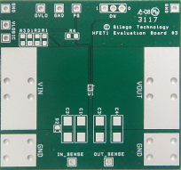
SLG59H1313C Evaluation Board
The SLG59H1313C-EVB board evaluates the SLG59H1313C High Voltage GreenFET, Load Switch.
For details on how to use the evaluation board, please refer to the evaluation board user manual included in the datasheet.
Filters
Applied Filters
Software & Tools
Filter by Type
Filter by Provider
Sample Code
Filter by Application
Filter by Function
Filter by Compiler
Filter by IDE
Simulation Models
Partner Solutions
No Results Found.
Make sure all keywords are spelled correctly.
Try fewer, different, or more general terms to vary your search.
If you have filters applied, consider deselecting some to broaden your results.
- Search our extensive knowledgebase, designed to help customers with their FAQs.
- Get help from our expert Renesas technical staff and community on our support forums.
Software & Tools (6)
No Results Found.
Make sure all keywords are spelled correctly.
Try fewer, different, or more general terms to vary your search.
If you have filters applied, consider deselecting some to broaden your results.
- Search our extensive knowledgebase, designed to help customers with their FAQs.
- Get help from our expert Renesas technical staff and community on our support forums.
A detailed overview of the GreenFET product line, focusing on the advantages of Renesas’ proprietary CuFET™ architecture and its impact on performance, size, and reliability. The presentation covers key specifications such as low RDS(on), high continuous current capability, and integrated protection functions including current limiting, thermal shutdown, and reverse‑current blocking. The session also outlines how GreenFET devices streamline power sequencing and reduce external component requirements.

Support Communities


