Features
- PCIe Gen 1–4 compliant
- Integrated terminations provide 100Ω differential Zo: reduced component count and board space
- 1.8V operation: reduced power consumption
- OE# pins: support DIF power management
- LP-HCSL differential clock outputs: reduced power and board space
- Programmable slew rate for each output: allows tuning for various line lengths
- Programmable output amplitude: allows tuning for various application environments
- DIF outputs are blocked until PLL is locked: clean system start-up
- Selectable 0%, -0.25%, or -0.5% spread on DIF outputs: reduces EMI
- External 25MHz crystal; supports tight ppm with 0ppm synthesis error
- Configuration can be accomplished with strapping pins: SMBus interface is not required for device control
- 3.3V tolerant SMBus interface works with legacy controllers
- Space-saving 4mm x 4mm 24-pin VFQFPN; minimal board space

Description
The 9FGV0241 is a 2-output very low power frequency generator for PCIe Gen 1–4 applications with integrated output terminations providing Zo = 100Ω. The device has two output enables for clock management and supports two different spread spectrum levels in addition to spread off.
Parameters
| Attributes | Value |
|---|---|
| Diff. Outputs | 2 |
| Diff. Output Signaling | LP-HCSL |
| Output Freq Range (MHz) | 25 - 25, 100 - 100 |
| Power Consumption Typ (mW) | 45 |
| Supply Voltage (V) | 1.8 - 1.8 |
| Output Type | LP-HCSL, LVCMOS |
| Xtal Freq (MHz) | 25 - 25 |
| Diff. Termination Resistors | 0 |
| Package Area (mm²) | 16 |
| Battery Backup | No |
| Battery Seal | No |
| CPU Supervisory Function POR | No |
| Crystal Frequency Trimming | No |
| Frequency Out Pin | No |
| Inputs (#) | 1 |
| Input Freq (MHz) | 25 - 25 |
| Function | Generator |
| Input Type | Crystal, LVCMOS |
| Core Voltage (V) | 1.8 |
| Output Voltage (V) | 0.8V, 1.8V |
| Product Category | PCI Express Clocks |
Package Options
| Pkg. Type | Pkg. Dimensions (mm) | Lead Count (#) | Pitch (mm) |
|---|---|---|---|
| VFQFPN | 4.0 x 4.0 x 0.9 | 24 | 0.5 |
Application Block Diagrams
 | Industrial Automation Platform with Arm Cortex-A53 This industrial automation platform is designed for Arm Cortex-A53 MPUs including the iMX8 series of application processors. |
 | Automated Optical Inspection (AOI) Powerful MPU with DRP-AI and Wi-Fi 6 support for high-speed, low-latency AOI systems. |
 | Smart Home Controller with Multiple PHYs All-in-one smart home gateway with multi-standard PHYs, intuitive control, and future-proof design. |
 | High-Performance Human Machine Interface (HMI) System Versatile system on module (SoM) for driving a wide range of human machine interface capabilities. |
Complete Your Design
Explore complementary products to elevate your design
Renesas Boards & Kits
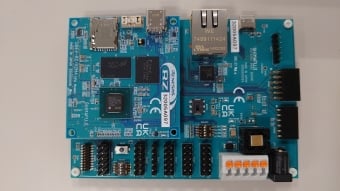
RZ/V2MA Evaluation Board Kit
This product is an evaluation board with RZ/V2MA configured as the key device. The RZ/V2MA Evaluation Board Kit is configured with the main board, base board, and option board (sold separately). The option board is used for PCIe evaluation.
This product supports the RZ/V2MA standard software... Read More
Partner Boards & Kits
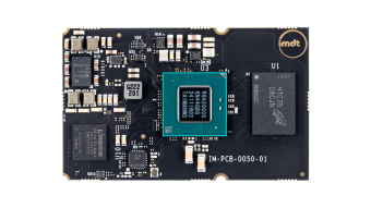
V2N System on Module (SoM)
Support Communities
-
RZV2M ISP integration issue
We have created a board based on the RZ/V2M processor. The only change we made compared to the RZV2M EVK is that we swapped the DDR data pins. We also made the necessary changes to the bootloader sources to accommodate these modifications. I am able to boot Linux ...
Oct 5, 2024 -
Separate Reference Clock on PCIe NVMe SSD
Hi, I have a PCIe design using Separate Reference Clock and the clock generator on end device side is Renesas 9FGV0241AKI.(see following picture of circuit architecture) The issue is that system cannot find NVMe SSD if using Separate Reference Clock. (System can find the NVMe SSD if using common ...
Jan 17, 2023 -
Separate Reference Clock on PCIe NVMe SSD
Hi, I have a PCIe design using Separate Reference Clock and the clock generator on end device side is Renesas 9FGV0241AKI.(see following picture of circuit architecture) The issue is that system cannot find NVMe SSD if using Separate Reference Clock. (System can find the NVMe SSD if using common ...
Jan 17, 2023

Support Communities


