
Features
- 1.8V/2.5V/3.3V flexible power rails
- Typical 150fs RMS 12kHz to 20MHz phase jitter
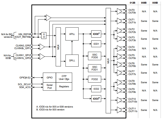
- 5/8/12 outputs with integrated crystal options
- 1kHz to 650MHz LVDS/LP-HCSL outputs
- 1kHz to 200MHz LVCMOS outputs
- Programmable hardware configuration select-pins
- PCIe Gen 5/6/7 ready
- Space saving packages 4mm × 4mm, 5mm × 5mm, 6mm × 6mm
- JESD204B/C support on differential or single-ended outputs with DC-coupling or AC-coupling
- Digital holdover and hitless switching
- Integrated crystal option for space saving and BOM optimization
- ITU-T G.8262 and G.82621 compliant for easy synchronized Ethernet application


Description
The RC31xxxB (RC31008B and RC31012B) are small form factor, fully integrated, low-power, high-performance jitter attenuators with network synchronization capabilities. The family supports JEDEC JESD204B/C for converter synchronization and SyncE for network-based synchronization. The RC31xxxB are ideal for driving converter circuits in wireless and wireline infrastructure, data center equipment, and instrumentation applications. The devices are members of Renesas' high-performance VersaClock® 7 family
Up to 27 configurations reusable across multiple designs may be stored in on-chip One-Time Programmable (OTP) memory or external I2C EEPROM. Redundant input is available for backup and used as a reference clock where needed.
Parameters
| Attributes | Value |
|---|---|
| Inputs (#) | 2 |
| Input Type | LVDS, LP-HCSL, LVCMOS |
| Product Category | VersaClock, IEEE 1588, Jitter Attenuators, Network Synchronization, PCI Express Clocks, Programmable Clocks |
| Diff. Outputs | 5, 8, 12 |
| Output Type | LVDS, LP-HCSL, LVCMOS |
| Output Voltage (V) | 1.8V, 2.5V, 3.3V |
| Input Freq (MHz) | 1 - 650 |
| Phase Jitter Typ RMS (ps) | 0.15 |
| Output Freq Range (MHz) | 0.001 - 650 |
| Fractional Output Dividers (#) | 3 |
| Core Voltage (V) | 1.8V, 2.5V, 3.3V |
| Output Banks (#) | 6 |
| Advanced Features | JESD204B/C, Spread Spectrum, Hitless Switching |
Applications
- Switches/Routers
- Synchronous Ethernet (SyncE) equipment
- Telecom Time Slave Clock (T-TSC) equipment
- Jitter attenuation for 10/25/40/100/200/400 Gbps Ethernet PHYs or switches
- Small cell for 4.5G and 5G