
Features
- Configurable OE pin function as OE, PD#, PPS, or DFC control function
- Configurable PLL bandwidth/minimizes jitter peaking
- PPS: Proactive Power Saving features save power during the end device power down mode
- PPB: Performance Power Balancing feature allows minimum power consumption based on the required performance
- DFC: Dynamic Frequency Control feature allows up to 4 different frequencies to switch dynamically
- Spread spectrum clock support to lower system EMI
- I2C interface
- Also supports crystal input
- Supported by Timing Commander™ software tool
- Available in AEC-Q100 qualified, Grade 2 (-40 °C to +105 °C) version

Description
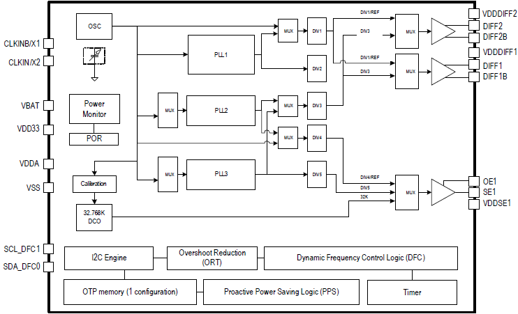
The 5P35021 is a VersaClock® programmable clock generator designed for low-power, consumer, and high-performance PCI Express applications. The 5P35021 device is a three-PLL architecture design, and each PLL is individually programmable allowing for up to five unique frequency outputs. The 5P35021 has built-in unique features such as Proactive Power Saving (PPS), Performance-Power Balancing (PPB), Overshoot Reduction Technology (ORT), and Extreme Low Power DCO. An internal OTP memory allows the user to store the configuration in the device without programming after powering up, and then program the 5P35021 again through the I2C interface.
The device has programmable VCO and PLL source selection to allow the user to do power-performance optimization based on the application requirements. It also supports one single-ended output and two pairs of differential outputs that support LVCMOS, LVPECL, LVDS, and LPHCSL. A low-power 32.768kHz clock is supported with only less than 5μA current consumption for the system RTC reference clock.
Parameters
| Attributes | Value |
|---|---|
| Diff. Outputs | 2 |
| App Jitter Compliance | PCIe Gen1, PCIe Gen2, PCIe Gen3 |
| Outputs (#) | 5 |
| Output Type | LVCMOS, LVPECL, LP-HCSL, LVDS |
| Output Freq Range (MHz) | 0.032768 - 500 |
| Input Freq (MHz) | 1 - 160 |
| Inputs (#) | 1 |
| Input Type | Crystal, LVCMOS, LVPECL, LVDS, LP-HCSL |
| Output Banks (#) | 3 |
| Core Voltage (V) | 3.3 |
| Output Voltage (V) | 1.8V, 2.5V, 3.3V |
| Feedback Input | No |
| Product Category | VersaClock 3S, Low Jitter Clocks (<700 fs RMS), Automotive Timing, General Purpose Clocks, PCI Express Clocks, Programmable Clocks |
| Selection Criteria | <700 fs RM |
Package Options
| Pkg. Type | Pkg. Dimensions (mm) | Lead Count (#) | Pitch (mm) |
|---|---|---|---|
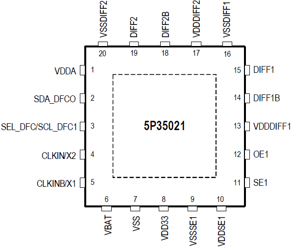
| VFQFPN | 3.0 x 3.0 x 1.0 | 20 | 0.4 |
Product Comparison
 | | | | |
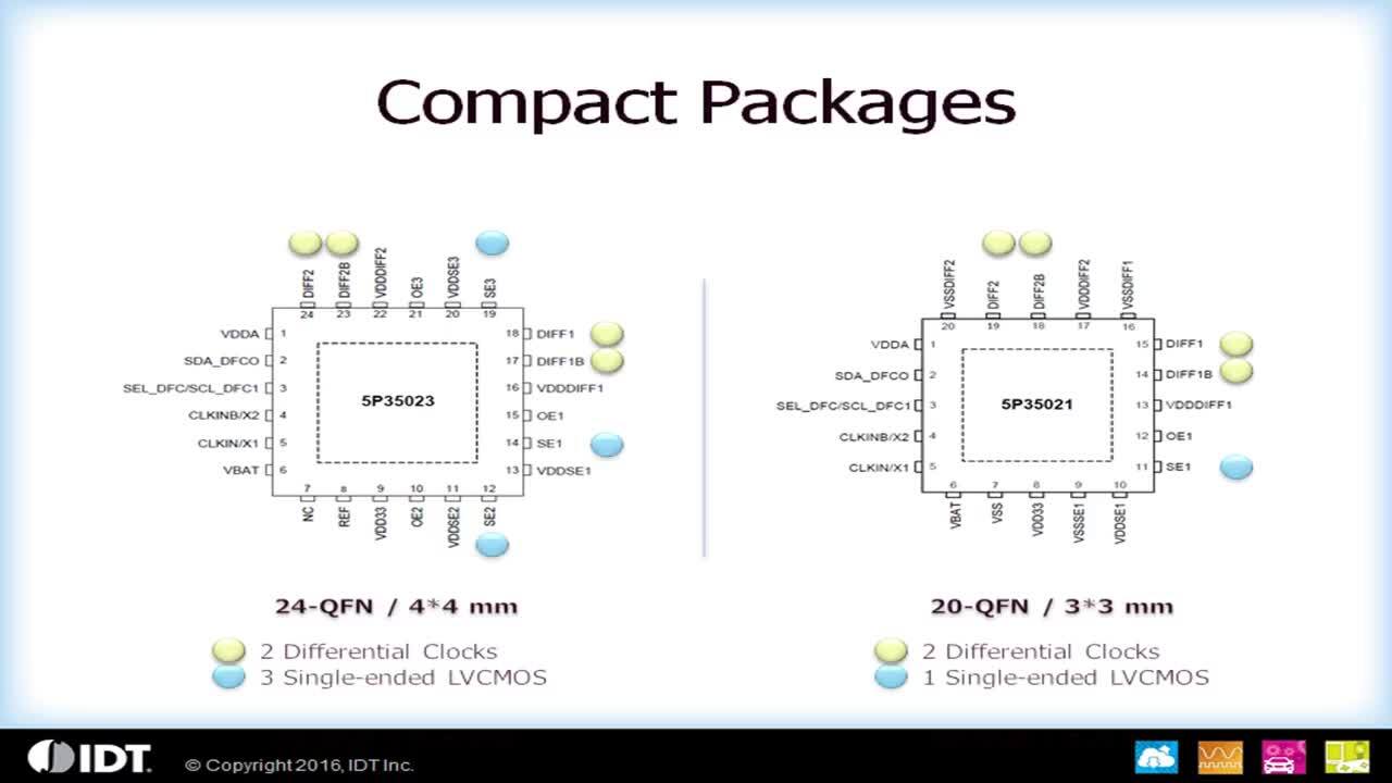
| 5P35021 | 5P35023 | 5L35021 | 5L35023 | |
| Outputs (#) | 5 | 7 | 5 | 7 |
| Output Type | LP-HCSL, LVCMOS, LVDS, LVPECL | LP-HCSL, LVCMOS, LVDS, LVPECL | LP-HCSL, LVCMOS | LP-HCSL, LVCMOS |
| Core Voltage (V) | 3.3 | 3.3 | 1.8 | 1.8 |
| Output Voltage (V) | 1.8, 2.5, 3.3 | 1.8, 2.5, 3.3 | 1.8 | 1.8 |
| Pkg. Dimensions (mm) | 3.0 x 3.0 x 1.0 | 4.0 x 4.0 x 0.9 | 3.0 x 3.0 x 1.0 | 4.0 x 4.0 x 0.9 |
Application Block Diagrams
 | Video Output Expansion for Surround View & AR HUD Integrated video output and AI for surround view and AR HUD with reduced cost and complexity. |
 | Power & Timing SoM for RZ/G2E Power and timing SoM ensures precise timing and efficient power distribution. |
Complete Your Design
Explore complementary products to elevate your design
Renesas Boards & Kits
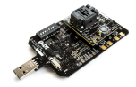
5P35021 VersaClock 3S Programmable Clock Development Kit
The DEV5P35021 programmable clock development kit is designed to support the 5P35021 VersaClock 3S device. It provides a convenient way of configuring and programming the blank parts for the 5P35021 device. With the onboard USB interface, the Timing Commander™ graphical user interface (GUI) can... Read More
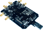
Programmer Board for VersaClock 3S - 5P3502x
The VersaClock® 3S-5P3502x programmer board is made to ease the programming of blank 5P35021 and 5P35023 devices. With the on-board USB interface, the Renesas Timing Commander™ graphical user interface (GUI) is used to communicate with the blank device in the socket for configuration and... Read More
Support Communities
-
5P35021申请定制料样品的流程
Hi,你好 我想用5P35021替代一个其他品牌的汽车buffer,这个过程会涉及定制料号。 我想知道申请定制料的流程要怎么走?另外具体 ...
Oct 31, 2025 -
5V49EE702NDGI8 vs 5V49EE702-097NDGI8
Hello.Could you please help to clarify tech details of difference 5V49EE702NDGI8 vs 5V49EE702-097NDGI8.I know that suffix -097 refers to Optional Dash Number (attached document). But I need more deep datails because 5V49EE702-097NDGI8 doesn't work well when i soldered it as replacement of 5V49EE702NDGI8. Thank you ...
Feb 8, 2024 -
I want to find a replacement for 844021BG-01LF, input 25MHz clock, output 125MHz LVDS clock
I want to find a replacement for 844021BG-01LF, input 25MHz clock, output 125MHz LVDS clock
Mar 9, 2022

Support Communities


