
Features
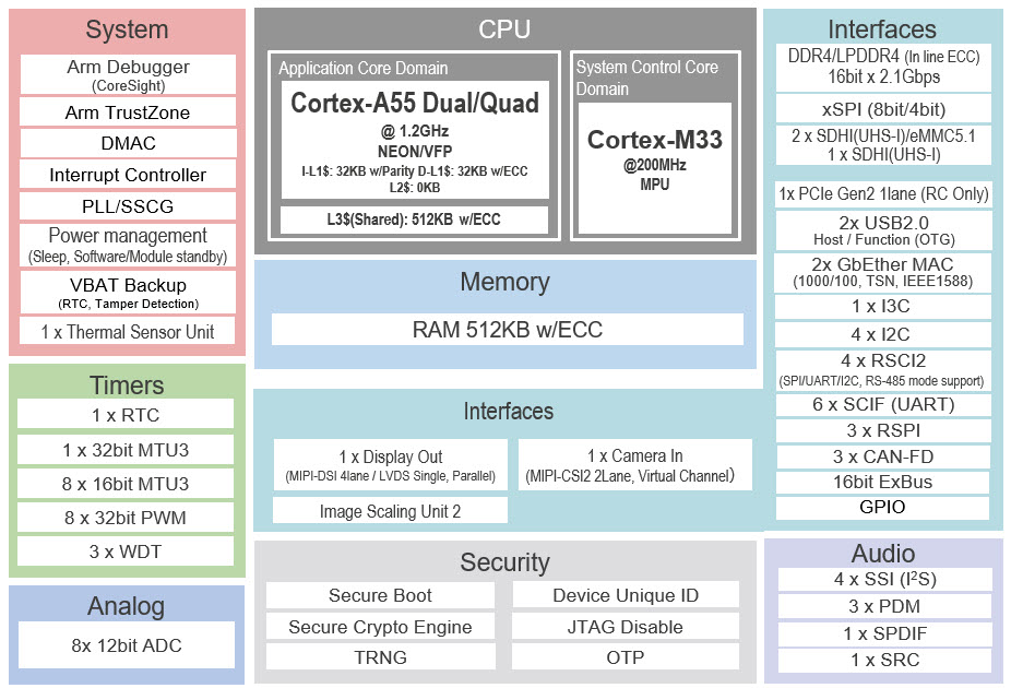
- Arm® Cortex®-A55 (quad or dual)
- Arm Cortex-M33
- Display interface (MIPI DSI, LVDS, or Parallel-IF)
- PCIe Gen2 1-lane
- USB 2.0 interface (2ch), SD interface (3ch)
- CAN interface (CAN FD)
- Gigabit Ethernet (2ch) with time-sensitive networking (TSN)
- Memory error detection and correction (ECC)
- LPDDR4 or DDR4 memory interface
- External bus interface
- Secure boot
- Secure update
- Hardware cryptographic IP
- True random number generator (TRNG)
- Secure debug
- Arm TrustZone®
- Tamper detection
- BGA package (14mm × 14mm, 17mm × 17mm)
- Explore the Renesas-validated DRAM Compatibility List
Description
The RZ/G3SE is a microprocessor (MPU) designed for IoT devices, integrating a quad-core CPU, a microcontroller core, a PCIe interface, and TSN-enabled Gigabit Ethernet on a single chip. With low-power standby capability and advanced security functions, the RZ/G3SE reduces system power consumption and improves reliability for IoT devices and edge computing applications. Robust hardware security protects IoT endpoints from cyberattacks. The built-in display interface is ideal for applications requiring display functionality. Full pin compatibility between the RZ/G3SE and RZ/G3L enables users to reuse the same PCB design and efficiently scale development across a wide range of applications, from display-equipped HMI devices to display-less IoT devices.
Parameters
| Attributes | Value |
|---|---|
| CPU Architecture | Arm |
| Main CPU | Cortex-A55 x 2 + Cortex-M33 x 1, Cortex-A55 x 4 + Cortex-M33 x 1 |
| Program Memory (KB) | 0 |
| RAM (KB) | 512 |
| Carrier Type | Bulk (Tray), Full Carton (Tray) |
| Supply Voltage (V) | 3 - 3.6 |
| I/O Ports | 113 |
| NPU | No |
| DRAM I/F | LPDDR4-2133/DDR4-2133 (16-bit) |
| 3D GPU | No |
| Temp. Range (°C) | Tj = -40 to +125 |
| Operating Freq (Max) (MHz) | 1200 |
| Ethernet speed | 10M/100M/1G |
| Ethernet (ch) | 2 |
| EtherCat (ch) (#) | 0 |
| USB FS (host ch/device ch) | ( 2 / 2 ) |
| USB HS (host ch/device ch) | ( 2 / 2 ) |
| USB SS (host ch/device ch) | ( 0 / 0 ) |
| PCI Express (generation and ch) | PCIe (Gen2.0 1Lane) x 1 ch |
| SCI or UART (ch) | 10 |
| SPI (ch) | 3 |
| I2C (#) | 4 |
| CAN (ch) | 3 |
| CAN-FD (ch) | 3 |
| Wireless | No |
| SDHI (ch) | 3 |
| High Resolution Output Timer | No |
| PWM Output (pin#) | 17 |
| 32-Bit Timer (ch) | 9 |
| 16-Bit Timer (ch) (#) | 8 |
| 8-Bit Timer (ch) | 0 |
| Standby operable timer | No |
| Asynchronous General Purpose Timer / Interval Timer (ch) | 0 |
| 16-Bit A/D Converter (ch) | 0 |
| 14-Bit A/D Converter (ch) | 0 |
| 12-Bit A/D Converter (ch) | 8 |
| 10-Bit A/D Converter (ch) | 0 |
| 24-Bit Sigma-Delta A/D Converter (ch) | 0 |
| 16-Bit D/A Converter (ch) | 0 |
| 12-Bit D/A Converter (ch) | 0 |
| 10-Bit D/A Converter (ch) (#) | 0 |
| 8-Bit D/A Converter (ch) | 0 |
| Capacitive Touch Sensing Unit (ch) | 0 |
| Graphics LCD Controller | No |
| MIPI Interfaces (DSI) (ch) | 1 |
| MIPI Interfaces (CSI) (ch) | 1 |
| Image Codec | No |
| Segment LCD Controller | No |
| Security & Encryption | AES, RSA, ECC, SHA-1, SHA-224/SHA-256, GHASH, TRNG |
Product Comparison
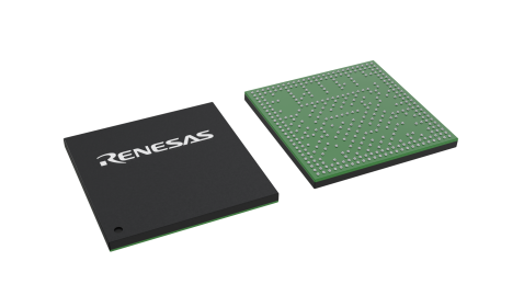 | | |
| RZ/G3SE | RZ/G3L | |
| CPU | Cortex-A55 x 2 + Cortex-M33 x 1, Cortex-A55 x 4 + Cortex-M33 x 1 | Cortex-A55 x 2 + Cortex-M33 x 1, Cortex-A55 x 4 + Cortex-M33 x 1 |
| 3D GPU | No | Arm Mali-G31 |
| Accelerator | No | Video Codec |
| Image Codec | No | H.264 |
| Pkg. Type | LFBGA | LFBGA |
Application Block Diagrams
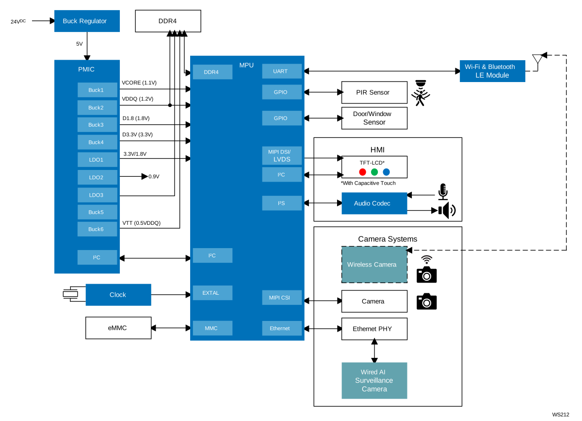 | AI-Enabled Smart Home Security Hub AI-enabled smart home security hub with edge-based video analytics, multi-sensor monitoring, and cloud connectivity for intelligent real-time threat detection. |