Features
- Optimized for Telecommunications Equipment, High‑performance Enterprise Computing, Motor Drives
- 18mΩ RDSON
- Maximum Continuous Current: 5A
- Wide Operating Supply Voltage: 4.5V to 13.2V
- Automatic nFET SOA Protection
- 3-Level, Pin-selectable VIN Overvoltage Lockout
- Capacitor-adjustable Inrush Current Control
- Two-stage Current Limit Protection:
- Resistor‑adjustable Active Current Limit
- Fixed 0.5A Short-circuit Current Limit
- ON-OFF Control: Active HIGH

Description
The SLG59H1120V is a high‑performance, self‑powered 18mΩ NMOS load switch designed for all 4.5V to 12V power rails up to 5A. Using a proprietary MOSFET design, the SLG59H1120V achieves a stable 18mΩ RDSON across a wide input voltage range and over temperature. In combining novel FET design and copper pillar interconnects, the SLG59H1120V package also exhibits a low thermal resistance for high‑current operation. Designed to operate over a -40 °C to 85 °C range, the SLG59H1120V is available in a low thermal resistance, RoHS‑compliant, 1.6mm x 3.0mm STQFN package.
Parameters
| Attributes | Value |
|---|---|
| FET Pass Device Type | Single N-Channel |
| VIN Channel 1 min. (V) | 4.5 |
| VIN Channel 1 max. (V) | 13.2 |
| Input Quiescent Current Channel 1, typ (µA) | 500 |
| Input Quiescent Current Channel 1, max (µA) | 600 |
| Input Quiescent Current when OFF Channel 1, typ (µA) | 1 |
| Input Quiescent Current when OFF Channel 1, max (µA) | 3 |
| RDSON (Typ) Channel 1 (mΩ) | 18 |
| IDS Channel 1 (A) | 5 |
| Enable | Active High |
| Output Voltage Slew Rate set by | Capacitor |
| Discharge Circuit | Yes |
| Undervoltage Protection | Yes |
| Over Voltage Protection | Yes |
| Power Good (PG), FAULT indicator | FAULT |
| Reverse current blocking | No |
| Reverse voltage detection | No |
| Over Current Protection (OCP) | Adjustable |
| Over Current Protection Setting Range Channel 1 | 1 - 5 |
| Short Circuit Protection | Yes |
| Over Temperature Protection (OTP) | Yes |
| Current Monitor Output | Yes |
| Internal TVS Surge Protection | No |
| Temp. Range (°C) | -40 to +85°C |
Application Block Diagrams
 | Ki Wireless Power Receiver System (Rx) High‑efficiency Ki receiver converting wireless power with integrated NFC to enable reliable, compact, cable‑free appliance operation. |
Additional Applications
- Enterprise Computing & Telecom Equipment 5V and 12V Point‑of‑Load Power Distribution
- PCI/PCIe Adapter Cards
- General-purpose High-voltage, Power-Rail Switching
- Multifunction Printers
- Fan Motor Control
Complete Your Design
Explore complementary products to elevate your design
Renesas Boards & Kits
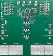
SLG59H1120V Evaluation Board
The SLG59H1120V-EVB board evaluates the SLG59H1120V High Voltage GreenFET, Load Switch.
For details on how to use the evaluation board, please refer to the evaluation board user manual included in the datasheet.
Support Communities
-
Richard
The SLG59H1120V datasheet shows a 400K resistor from the CAP pin to ground, in parallel with the slew rate cap. This resistor doesn't seem to be documented. What is it for and how critical is the value? In a current sharing scheme with two devices in parallel and a ...
Nov 22, 2021

Support Communities


