Features
- 2 power supply inputs:
- 2.5V (±8%) to 5.0V (±10%) VDD
- 3.3V (±9%) to 12.0V (±10%) VDD2
- 4 high-voltage high-current drive GPOs
- Dual/Single full-bridge driver option
- Quad/Dual/Single half-bridge driver option
- Slew rate modes:
- Motor driver mode
- Pre-driver (MOSFET driver) mode
- Sleep function
- Low RDS(ON) high-side + low-side resistance = 0.4Ω typical
- 2A peak, 1.5A RMS per full bridge (at VDD2 = 5V, TA = 25°C)
- 4A peak, 3A RMS per two full bridge connected in parallel (at VDD2 = 5V, TA = 25°C)
- 2A peak, 1.5A RMS per half bridge GPO (at VDD2 = 5V, TA = 25°C)
- Integrated overcurrent (OCP), short circuit, undervoltage-lockout (UVLO), thermal shutdown (TSD) protections
- SENSE_A, SENSE_B inputs that are connected to the current comparators for current control
- Fault signal indicator (OCP/UVLO/TSD)
- Differential amplifier with integrator and comparator for motor speed control function
- 2 current sense comparators with dynamical Vref mode
- 2 high-speed general-purpose ACMPs
- Modes: UVLO, OCP, TSD, voltage monitor, current monitor
- 1 voltage reference (Vref) output
- 5 multi-function macrocells
- 4 selectable DFF/LATCH/3-bit LUTs + 8-bit delay/counters
- 1 selectable DFF/LATCH/4-bit LUT + 16-bit delay/counter
- 12 combination function macrocells
- 3 selectable DFF/LATCH or 2-bit LUTs
- 1 selectable programmable pattern generator or 2-bit LUT
- 6 selectable DFF/LATCH or 3-bit LUTs
- 1 selectable pipe delay or ripple counter or 3-bit LUT
- 1 selectable DFF/LATСH or 4-bit LUT
- 2 PWM macrocells
- Flexible 8-bit/7-bit PWM mode with the duty cycle control
- 16 preset duty cycle registers switching mode for PWM Sine or other waveforms
- Serial communications
- I2C protocol interface
- Programmable delay with edge detector output
- Additional logic function – One deglitch filter with edge detectors
- 2 oscillators (OSC)
- 2.048kHz oscillator
- 25MHz oscillator
- Analog temperature sensor with ACMP connected output
- Power-on Reset (POR)
- One-time programmable memory
- Operating temperature range: -40°C to 105°C
- RoHS compliant/Halogen-free
- 20-pin STQFN: 2mm x 3mm x 0.55mm, 0.4mm pitch

Description
The SLG47105-E provides a small, low-power component for commonly used mixed-signal and bridge functions. The user creates their circuit design by programming the one-time programmable (OTP) non-volatile memory (NVM) to configure the interconnect logic, the IO pins, the high-voltage pins, and the macrocells of the SLG47105-E. Configurable PWM macrocells in combination with special high-voltage outputs will be useful for motor drive or load drive applications. High-voltage pins allow for the design of smart level translators or for driving the high-voltage high-current load.
Parameters
| Attributes | Value |
|---|---|
| Nominal VDD | 2.3 - 5.5 |
| VDD2 (V) | 3 - 13.2 |
| GPIOs (#) | 12 |
| Special Features | 2x CCMP, 2x H-/4x Half-Bridge, 2x PWM, Int&Diff Amp |
| ACMP Channels (#) | 2 |
| CNT/DLY (Max) (#) | 5 |
| Look-up Table (LUTs) | 17 |
| D Flip-flops (DFFs) (#) | 15 |
| Pipe Delay | 16-stage |
| # of Programable Delays (#) | 1 |
| Oscillator Type | LF OSC, Ring OSC |
| Temperature Sensor (ch) (#) | 1 |
| Temp. Range (°C) | -40 to +105°C |
| Interface | I2C |
| Memory Type | OTP |
Package Options
| Pkg. Type | Pkg. Dimensions (mm) | Lead Count (#) | Pitch (mm) |
|---|---|---|---|
| TQFN | 2.0 x 3.0 | 20 | 0.4 |
Applications
- Outdoors electronics
- Factory automation
- E-Bikes
- Power electronics
- EV charging stations
- Personal computers and servers
- Motor drivers
- High-voltage MOSFET drivers
- LED matrix dimmers
Renesas Boards & Kits
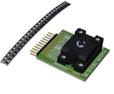
GreenPAK SLG47105-EV Development Kit with Socket Adapter
The SLG47105EV-SKT is a socket adapter kit for use with the SLG4DVKADV GreenPAK™ Advanced Development Board or SLG4DVKLITE GreenPAK Lite Development Board. The SLG47105EV-SKT kit includes the SLG4SA20HV-20x30 socket adapter and 50 SLG47105-EV HVPAK™ programmable mixed-signal matrix IC... Read More
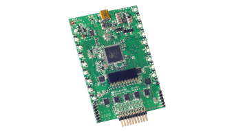
GreenPAK Advanced Development Board
The GreenPAK™ Advanced Development Board provides full programming, emulation, and testing functions for the GreenPAK programmable mixed-signal devices - for use with SLG46xxxX-SKT/SLG47xxxV-SKT socket kits.
The board works in tandem with the GreenPAK Designer software (built into the Go... Read More
Test This Board Remotely

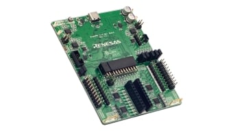
GreenPAK Lite Development Board
The GreenPAK™ Lite Development Board provides full programming, emulation, and testing functions for GreenPAK devices, working in conjunction with the Go Configure™ Software Hub. Board functionality is provided by the RX66T MCU from Renesas.
GreenPAK Introduction Kit Lite
The SLG4DVKLITEINTRO-KIT is an all-in-one development kit designed for engineers and developers starting new projects with GreenPAK™ programmable mixed-signal ICs. The kit includes the SLG4DVKLITE Lite Development Board with USB cable and ten DIP proto boards (SLG46120V-DIP, SLG46721V-DIP,... Read More
Support Communities
-
SLG47105 exposure pad layout recommedation
We are using SLG47105V, how the exposure pads should be connected to ground? Any vias required there are can we connect it to gnd-pin on top layer? Can we connect general gnd and HV GND pads?
Oct 7, 2025 -
SLG47105V emulation (External)
Hello, I am trying to debug a SLG47105V. I have connected SCL and SDA from the GreenPak Advanced development board to the external chip and have selected 'external 0001' as Device. The SLG47105V is powered correctly When pressing Emulation, everthing goes fine, no error, but somehow the chip is not ...
Mar 25, 2022 -
SLG47105 for small motor drive and control loop.
The image is to show my plan to use a SLG47105 for a small motor driver with control loop to rotate the shaft between 0-90° at 17Hz sinusoidal. What platform should I purchase for the development? Thanks, LaszloeeHi Laslozee, That you for your appeal, SLG47105 can be used for ...
Sep 8, 2021

Support Communities


