Power designers continue to face the familiar challenge of how to deliver more power in less space without sacrificing efficiency or creating a thermal problem. Achieving this is especially important in 48V architectures, where the intermediate bus often must be stepped down efficiently to 12V or lower rails.
In this scenario, questions arise around what happens when a designer increases the switching frequency to reduce passive component size. With conventional Si MOSFETs, the resulting switching losses can reduce efficiency and increase thermal challenges, leading to the question of whether low-voltage GaN can provide the additional design margin needed to improve this trade-off.
Evaluating Low-Voltage GaN in a 48V to 12V Power Platform
To answer this question, we evaluated a practical 48V to 12V DC/DC converter and compared measured results from GaN and Si MOSFET implementations. For this evaluation, we used a synchronous buck converter based on two Renesas RTP100E005G1FL 100V, 5mΩ GaN FETs and the RRP68150 half-bridge GaN gate driver, as shown in Figure 1. The EVB-RTP100E005G1FL evaluation board integrates power devices, a gate driver, an inductor, input and output capacitors, and accessible measurement points. This provides a practical platform for evaluating efficiency, power loss, switching behavior, and thermal performance. Figure 2 shows the 3.3mm x 3.3mm FCLGA package of the GaN FET.
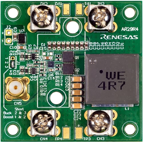
Figure 1. RTP100E005G1FL 48V to 12V synchronous buck evaluation platform
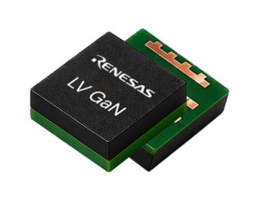
Figure 2. Renesas REXGaN low-voltage GaN FET
| Parameter | Evaluation Condition |
|---|---|
| Input Voltage | 48V DC |
| Output Voltage | 12V DC |
| Maximum Output Current | 18A |
| Switching Frequencies for Comparison | 150kHz, 250kHz, and 500kHz |
| Inductor | 4.7µH |
| GaN FET | RTP100E005G1FL, 100V, 5.0mΩ |
| Gate Driver | RRP68150 |
The on-state resistance of a power switch is an important contributor to conduction loss, but it is not the only factor affecting conversion efficiency. Switching performance is also influenced by gate charge, gate-drain charge, output charge, reverse-recovery behavior, switching speed, dead time, and the parasitic elements in the power loop.
The measured comparison used the 100V, 5.0mΩ GaN FET and a commercially available 80V, 5.2mΩ Si MOSFET in a similar 3.3mm x 3.3mm package. This creates a useful comparison because the nominal on-resistance and footprint are closely matched, and the evaluation hardware is identical except for the FETs. This lets us accurately observe the impact of switching-related characteristics.
| Parameter | Renesas Low-Voltage GaN | Comparable Si MOSFET |
|---|---|---|
| VDS Rating | 100V | 80V |
| RDS(on) (typ.) | 5.0mΩ | 5.2mΩ |
| Qg (typ.) | 5.2nC | 19nC |
| Qgd (typ.) | 1nC at 50V | 6.4nC at 40V |
| Qoss (typ.) | 24.2nC at 50V | 39nC at 40V |
| Qrr (typ.) | 0nC | 129nC |
The GaN device requires less gate charge to switch, stores less output charge, and has no conventional body diode reverse-recovery charge. These characteristics help reduce driver effort and switching-related energy loss, while supporting shorter dead time. The benefit grows as switching frequency increases, helping explain the widening efficiency and temperature advantage shown in the measurements.
GaN Pulls Ahead as Switching Frequency Rises
Our experts evaluated the GaN and Si MOSFET implementations in the same 48V to 12V buck-converter platform at 150kHz, 250kHz, and 500kHz, using a 4.7µH inductor. The efficiency curves in Figure 3 indicate that the two solutions are relatively close at 150kHz.
At 250kHz, the GaN implementation begins to establish a clearer advantage, and at 500kHz, the efficiency gap becomes more significant across much of the measured load range. At an output current of 16A, this advantage delivers approximately 3.2W lower power loss than the comparable Si MOSFET.
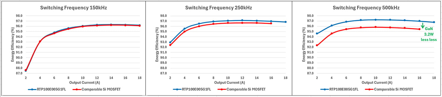
Figure 3. Measured efficiency comparison at 150kHz, 250kHz, and 500kHz
This trend is more informative than any single peak-efficiency value. At lower frequencies, conduction loss and passive component loss represent a larger share of total loss, so two devices with similar RDS(on) show similar results. As switching frequency rises, the effects of switching characteristics become more significant. The measured curves illustrate how GaN can provide higher efficiency as the converter operates at higher frequencies.
The thermal measurements in Figure 4 show a trend consistent with the efficiency comparison. At 150kHz, the temperature difference between the GaN and Si MOSFET solutions is relatively small. As the switching frequency increases to 250kHz and 500kHz, the lower temperature of the GaN solution becomes more apparent. At 500kHz and an output current of 10A, the measured temperature of the comparable Si MOSFET reaches approximately 104°C; GaN is 22°C cooler.
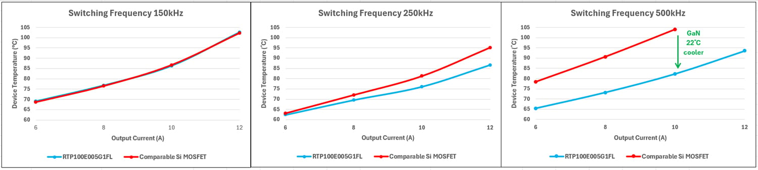
Figure 4. Measured device temperature comparison at 150kHz, 250kHz, and 500kHz
Figure 5 further characterizes the EVB-RTP100E005G1FL board in terms of efficiency and total power loss over output current at multiple switching frequencies. Under the specific conditions of this evaluation platform, the 500kHz operating point delivers the highest measured efficiency. A small difference in conversion efficiency can represent a meaningful difference in power dissipation. Lower total loss can reduce semiconductor temperature, ease cooling requirements, create additional thermal margin or allow a designer to increase switching frequency while maintaining an acceptable efficiency target.
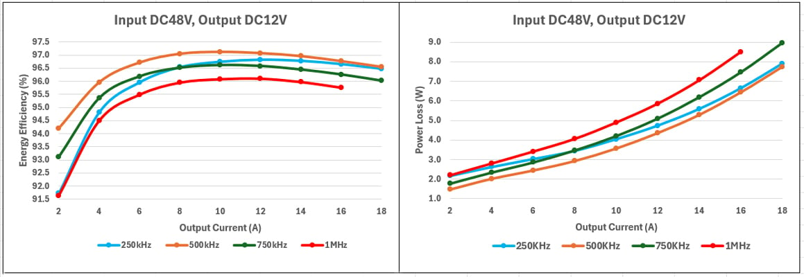
Figure 5. EVB-RTP100E005G1FL efficiency and total power loss trends vs. load and switching frequency
How to Use GaN's High-Frequency Advantage in Practical Designs
Increasing switching frequency can reduce the energy storage requirement of passive components and enable a smaller converter form factor. However, with Si MOSFETs, higher switching frequencies generally result in greater switching losses, reducing efficiency and increasing thermal challenges. The measured comparison shows that low-voltage GaN changes this trade-off by reducing the efficiency penalty at higher frequencies.
Depending on the system design objectives, designers can choose from the following approaches:
- Maintain the original switching frequency and use the loss reduction to improve efficiency and thermal margin.
- Increase the switching frequency to reduce passive component size, while optimizing trade-offs between efficiency, temperature, EMI, component size, and cost for specific system requirements.
This flexibility is one of the most important system-level benefits of low-voltage GaN. It does not mean that every GaN design should operate at the maximum possible frequency, but it gives engineers a wider and more useful optimization range.
Realizing GaN's device-level advantages requires an optimized power stage rather than a simple Si MOSFET replacement. The gate driver should be placed close to the GaN FETs, turn-on and turn-off paths should be controlled, and common source and power loop inductance should be minimized. Dead time must also be tuned to balance third-quadrant conduction loss against cross-conduction risk.
Measurement technique matters, as well. High-inductance probing can distort VGS and VDS waveforms and can make ringing appear worse than it is at the device terminals. The evaluation board addresses these practical needs with a compact four-layer layout, the RRP68150 driver, and dedicated measurement points.
Increased Efficiency and Performance with GaN
The 48V to 12V synchronous buck testing results show that the RTP100E005G1FL device delivers a growing efficiency advantage over the comparable Si MOSFET as switching frequency increases, despite the devices having similar nominal on-resistance and package size. This result demonstrates how GaN switching characteristics translate into system-level performance.
One of the key takeaways from this evaluation is that low-voltage GaN gives power designers more room to optimize. Instead of treating higher switching frequency only as an efficiency penalty, engineers can use it as a design lever to improve efficiency, create thermal margin, reduce passive-component size, or balance these benefits to best suit the application.
The RTP100E005G1FL is part of the broader REXGaN 100V GaN family. Lower-resistance options, including 2.6mΩ, 1.8mΩ, and 1.2mΩ devices and their evaluation platforms extend the available choices for higher current and lower conduction loss designs. The 1.8mΩ and 1.2mΩ come in dual-side cooled packages to help designers remove the heat from both sides of the device, increasing the power handling capability significantly. The exposed substrate of the GaN devices reduces RΘJCT down to 0.2°C/W.
For additional design information, please see the Renesas low-voltage GaN portfolio, RRP68150 GaN gate driver, and EVB-RTP100E005G1FL evaluation board documentation, including schematics, layout guidance, test conditions, and measured performance data.