Features
- Dense array of configurable logic
- 2240 5-bit LUTs
- 2240 D-type flip flops (DFFs)
- 10kb distributed memory
- 64kb block random access memory (BRAM)
- Power supply domains
- Two separate domains (20 GPIOs per domain)
- VDDIO0 and VDDIO1: 1.71V to 3.465V
- VDDC: 1.1V ± 5%
- Clocking
- High-frequency oscillator
- 50MHz high-frequency oscillator
- Oscillator post divider
- Divide oscillator clock by a power of 2 (range 1 to 128)
- Two independent outputs
- Phase-locked loop (PLL)
- Input from an external source, internal oscillator, or LVDS differential clock
- High-frequency oscillator
- Power-on reset (POR)
- Flexible power-consumption control
- FPGA core power control
- Clock sources power control
- BRAM deep-sleep/power-gated modes
- General-purpose IOs
- 40 GPIOs
- Flexible configuration options
- Selectable drive strength (4/8/12mA)
- Optional pull-up – 1x or 2x
- Optional pull-up control from the FPGA core
- Optional Schmitt trigger input
- Six LVDS-capable GPIOs (three true-LVDS pairs up to 100Mbps)
- Fast routing capability between pairs of GPIO located in different IO voltage domains
- Bitstream security features
- CRC integrity check
- AES decryption
- Configuration options
- OTP mode – Load from built-in OTP memory
- SPI Controller (Master) mode – Load from external Flash memory
- SPI Target (Slave) mode – Load from external source (MCU host)
- Boot control logic: Can address up to 16 different bitstreams from external memory
- Two idle low-power modes
- Sleep mode when configuration is being retained and no device re-configuration is needed
- Reset mode when device re-configuration is required after exit from this mode
- Possibility to retain GPIOs and BRAM states in both low-power modes
- Low power consumption in both modes (< 85µA)
- Operating temperature range: -40°C to 85°C
- RoHS-compliant/Halogen-free
- Available packages
- SLG47921V: 48-pin LQFN, 6.0mm x 6.0mm, 0.4mm pitch
- SLG47921C: 48-pin WLCSP, 3.24mm x 2.57mm, 0.35mm pitch

Description
The SLG47921 is a small, low-power device for common FPGA applications. Users create a circuit design by programming the one-time programmable (OTP) non-volatile memory (NVM) or providing a bitstream through an SPI interface to configure the FPGA core, the IO pins, and the macrocells of the chip. This highly versatile device enables a wide range of FPGA applications.
Parameters
| Attributes | Value |
|---|---|
| Vddc | 1.05 - 1.15 |
| Vddio | 1.71 - 3.465 |
| GPIOs (#) | 40 |
| Look-up Table (LUTs) | 2240 |
| D Flip-flops (DFFs) (#) | 2240 |
| BRAM (kbit) | 64 |
| Distributed Memory (kbit) | 10 |
| Vddio Domains (#) | 2 |
| LVDS Channels (#) | 3 |
| On-chip Oscillator | Yes |
| On-chip Oscillator Freq. | 50MHz / 3MHz |
| PLLs | 2 |
| Configuration Modes | SPI Controller, SPI Target, OTP |
| Memory Type | OTP |
| Temp. Range (°C) | -40 to +85°C |
| Sleep/Reset Mode Current (µA) | 77 |
| Static State Iddc (µA) | 118 |
| Special Features | Sleep Mode,Fast Route,Bitstream AES Decryption,Boot Control |
Application Block Diagrams
 | Handheld Analog Gaming Console Analog gaming console with hardware-accurate emulation of classic systems and minimal input latency. |
Additional Applications
- Consumer electronics
- Data communications equipment
- Handheld and portable electronics
- Notebooks and tablet PCs
- Industrial instrumentation and control
Complete Your Design
Explore complementary products to elevate your design
Renesas Boards & Kits
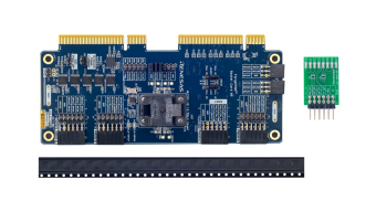
ForgeFPGA SLG47921C Socket Card Kit
The SLG47921C-SKT is a socket card kit for use with the SLG4DVKGOCONF Go Configure Development Board. The SLG47921C-SKT kit includes the ForgeFPGA™ Socket Card #5 (SLG7SC5), 20 samples of SLG47921C, and a Pmod™ LED adapter.
The ForgeFPGA Socket Card #5 is a development board designed for... Read More
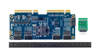
ForgeFPGA SLG47921V Socket Card Kit
The SLG47921V-SKT is a socket card kit for use with the SLG4DVKGOCONF Go Configure Development Board. The SLG47921V-SKT kit includes the ForgeFPGA™ Socket Card #3 (SLG7SC3), 20 samples of SLG47921V, and a Pmod™ LED adapter.
The ForgeFPGA Socket Card #3 is a development board designed for... Read More
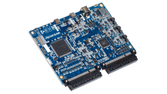
Go Configure Development Board
The Go Configure™ Development Board is a universal development board for Renesas' ForgeFPGA products that supports all features of the Go Configure™ Software Hub. A set of compatible socket cards is available for a quick and easy start to the development process. This board is ideal for rapid... Read More

ForgeFPGA GameBuddy Reference Design
The ForgeFPGA™ GameBuddy reference design demonstrates the flexibility of Renesas products through an interactive gaming platform featuring:
- Main Menu and Presentation Mode: Enables QSPI communication with SPI Flash and transitions between configurations using internal reset.
- Ping-Pong with FPGA:... Read More
Knowledge Base
-
What drive strength options are available for GPOs?
Last Updated: 03/25/2026 Question: What drive strength options are available for GPOs? Answer: In SLG47910 two drive strength options available: 4/8 mAIn SLG47912, SLG47920, SLG47921 three drive strength options available - 4/8/12 mA Suitable Products ForgeFPGA™
Mar 25, 2026 -
Is it possible to initialize the BRAM block?
Last Updated: 03/25/2026 Question: Is it possible to initialize the BRAM block? Answer: BRAM initialization is not supported on the SLG47910. However, it is supported on the SLG47912, SLG47920, and SLG47921. Suitable Products ForgeFPGA™
Mar 25, 2026 -
How much SPI Flash memory is required to store the ForgeFPGA™ bitstream?
Last Updated: 03/25/2026 Question: How much SPI Flash memory is required to store the ForgeFPGA bitstream? Answer: The SLG47910 requires 384 kbit of memory, while the SLG47912, SLG47920 and SLG47921 require 769 kbit. Suitable Products ForgeFPGA
Mar 25, 2026

Support Communities


