
Features
- Ultra-fast switching e-mode GaN HEMT
- JEDEC-qualified GaN technology
- Silicon-compatible package footprint for easy design migration
- Low 1.8mΩ typical on-resistance
- Dual-side-cooled package for simplified thermal design
- Zero reverse recovery charge (Qrr)
- Low gate charge and output charge for improved efficiency
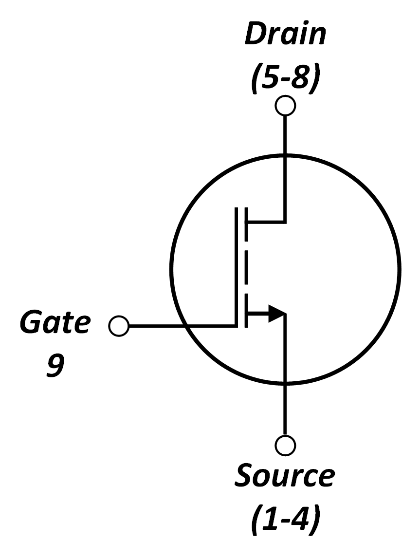
Description
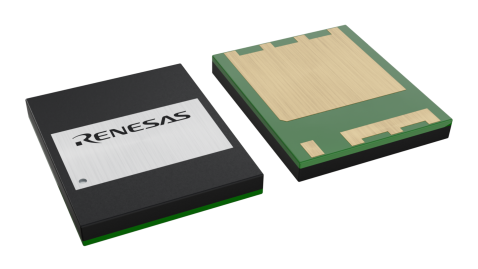
The RTP100E1P8G1FL-DSC is a 100V, 1.8mΩ enhancement-mode (e-mode) gallium nitride (GaN) FET built on Renesas' Gen 1 REXGaN® platform and housed in a compact 3.3mm × 3.3mm dual-side-cooled (DSC) FCLGA package. Utilizing advanced packaging technology, it combines ultra-fast switching performance with enhanced thermal characteristics to enable high-efficiency, high-power-density designs. Its dual-side-cooled package and silicon-compatible footprint simplify migration from traditional silicon MOSFETs to GaN technology, helping reduce development time, improve thermal management, and lower overall power losses.
Parameters
| Attributes | Value |
|---|---|
| Blocking Capability | Uni-Directional Switch |
| Qualification Level | Standard |
| Vds min (V) | 100 |
| V(TR)DSS max (V) | 120 |
| RDSON (Typ) (mΩ) | 1.8 |
| Vth typ (V) | 1.1 |
| Id max @ 25°C (A) | 36.7 |
| Qg typ (nC) | 16.3 |
| Qoss (nC) | 55 |
| Ron * Qoss (FOM) | 99 |
| Ciss (Typical) (pF) | 1980 |
| Coss (Typical) (pF) | 600 |
| Mounting Type | Surface Mount |
| Temp. Range (°C) | -40 to +150°C |
Package Options
| Pkg. Type | Pkg. Dimensions (mm) | Lead Count (#) | Pitch (mm) |
|---|---|---|---|
| FCLGA | 3.3 x 3.3 x 0.796 | 9 | 0.65 |
Product Comparison
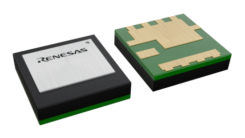 | 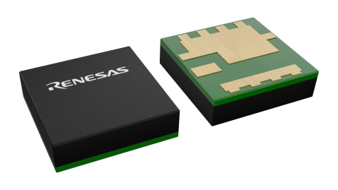 | 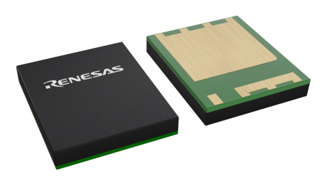 |  | |
| RTP100E1P8G1FL-DSC | RTP100E005G1FL | RTP100E2P6G1FL | RTP100E1P2G1FL-DSC | |
| RDSON (Typ) (mΩ) | 1.8 | 5 | 2.6 | 1.2 |
| Theta-JA (°C/W) | 47 | 45 | 29.4 | 18.4 |
| IDS (A) @ Ta = 25°C | 29 | 17 | 30 | 57 |
| IDS (A) @ Tc = 25°C | 282 | 59 | 109 | 545 |
| Qoss (nC) | 55 | 24.2 | 46 | 86 |
| Qg typ (nC) | 16.3 | 5.2 | 9.4 | 27 |
| Pkg. Type | FCLGA | FCLGA | FCLGA | FCLGA |
| Pkg. Dimensions (mm) | 3.3 x 3.3 x 0.796 | 3.3 x 3.3 x 0.902 | 5.0 x 6.0 x 0.902 | 5 x 6 x 0.702 |
Application Block Diagrams
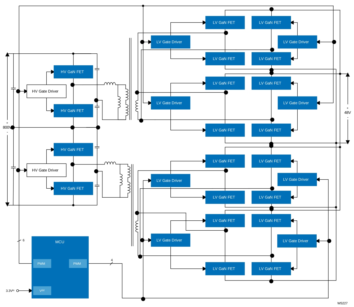 | 800V to 48V DCX System Efficiently converts an 800V DC bus to 48V DC with galvanic isolation for high-density, high-efficiency power delivery. |
Additional Applications
- 48V Intermediate Bus Converters for Telecom and AI Data Centers
- Synchronous Rectification and DC/DC Converters
- Battery-Powered Tools
- Class-D Audio Amplifiers
- Energy Storage Systems
- 48V Servo Drive
- Robotics Systems