
Features
- 1.8V/2.5V/3.3V flexible power rails
- -40° to +105°C ambient operating temperature
- Typical 102fs RMS 12kHz-20MHz
- 9/12 outputs
- 8kHz to 650MHz LP-HCSL outputs
- 8kHz to 200MHz LVCMOS outputs
- Programmable hardware configuration select-pins
- PCIe® Gen7 Common Clock jitter: 4.2fs RMS (typ.)
- PCIe Common Clock (CC) and Independent Reference clock (IR) support
- PCIe Gen 5/6/7 ready
- Space saving packages 5mm × 5mm, 6mm × 6mm
- 1V, 1.8V, 2.5V, and 3.3V LVCMOS outputs
- Internal OTP holds up to 18 configurations
Description
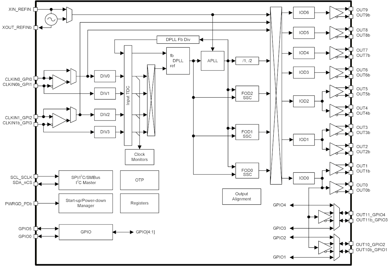
The RC313xxA (RC31312A and RC31309A) is a member of Renesas' VersaClock® 8 programmable clock generator/jitter attenuator family. The device is comprised of a programmable fractional-N DPLL for ultra-low phase noise clocking and jitter attenuation, and an Analog PLL (APLL) driving three independent programmable fractional output dividers (FOD) and individual IODs on each of the seven output banks. The devices can simultaneously provide low-phase jitter non-spreading clocks for Ethernet and storage applications and spread-spectrum PCIe Gen7 clocks.
Up to 18 configurations reusable across multiple designs may be stored in on-chip One-Time Programmable (OTP) memory or external I2C EEPROM. Redundant input is available for backup and used as a reference clock where needed.
Parameters
| Attributes | Value |
|---|---|
| Inputs (#) | 2 |
| Input Type | LVCMOS, CML, LVDS, HCSL, LVPECL, Crystal |
| Product Category | VersaClock, Jitter Attenuators, Network Synchronization, PCI Express Clocks, Programmable Clocks |
| Diff. Outputs | 9, 12 |
| Output Type | LVDS, LP-HCSL, LVCMOS, LVPECL |
| Output Voltage (V) | 1.8V, 2.5V, 3.3V |
| Input Freq (MHz) | 650, 150 |
| Output Freq Range (MHz) | 0.008 - 650 |
| Fractional Output Dividers (#) | 3 |
| Core Voltage (V) | 1.8V, 2.5V, 3.3V |
| Output Banks (#) | 6, 7 |
| Advanced Features | Spread Spectrum, Hitless Switching |
Product Comparison
 |  | | |
| RC313 | RC210 | RC310 | |
| Diff. Outputs | 9, 12 | 5, 8, 12 | 5, 8, 12 |
| Output Type | LP-HCSL, LVCMOS, LVDS, LVPECL | LP-HCSL, LVCMOS, LVDS | LP-HCSL, LVCMOS, LVDS |
| Output Voltage (V) | 1.8, 2.5, 3.3 | 1.8, 2.5, 3.3 | 1.8, 2.5, 3.3 |
| Input Freq | 0.000000 - 150.000000, 0.000000 - 650.000000 | 1.000000 - 650.000000 | 1.000000 - 650.000000 |
| Core Voltage (V) | 1.8, 2.5, 3.3 | 1.8, 2.5, 3.3 | 1.8, 2.5, 3.3 |
| App Jitter Compliance | PCIe Gen1, PCIe Gen2, PCIe Gen3, PCIe Gen4, PCIe Gen5, PCIe Gen6, PCIe Gen7 | PCIe Gen1, PCIe Gen2, PCIe Gen3, PCIe Gen4, PCIe Gen5, PCIe Gen6, PCIe Gen7 | PCIe Gen1, PCIe Gen2, PCIe Gen3, PCIe Gen4, PCIe Gen5, PCIe Gen6, PCIe Gen7 |
| Phase Jitter Typ RMS (fs) | 102 | 150.000 | 150.000 |
| Temp. Range (°C) | -40 to 105°C | -40 to 85°C | -40 to 85°C |
Applications
- Reconfigurable High-Performance Clocking System
- Power & Timing System for AI Accelerator Card