Features
- Configurable OE pin function as OE, PD#, PPS, or DFC control function
- Configurable PLL bandwidth/minimizes jitter peaking
- PPS: Proactive Power Saving features save power during the end device power down mode
- PPB: Performance Power Balancing feature allows minimum power consumption based on required performance
- DFC: Dynamic Frequency Control feature allows up to 4 different frequencies to switch dynamically
- Spread spectrum clock support to lower system EMI
- I2C interface
- Also supports crystal input
- Supported by the Timing Commander™ software tool
- Available in AEC-Q100 qualified, Grade 2 (-40 °C to +105 °C) version


Description
The 5P35023 is a VersaClock® programmable clock generator designed for low-power, consumer, and high-performance PCI Express applications. The 5P35023 device is a three-PLL architecture design, and each PLL is individually programmable and allows for up to five unique frequency outputs. The 5P35023 has built-in unique features such as Proactive Power Saving (PPS), Performance-Power Balancing (PPB), Overshot Reduction Technology (ORT), and Extreme Low Power DCO. An internal OTP memory allows the user to store the configuration in the device without programming after powering up, and then program the 5P35023 again through the I2C interface.
The device has programmable VCO and PLL source selection to allow the user to do power-performance optimization based on the application requirements. It also supports three single-ended outputs and two pairs of differential outputs that support LVCMOS, LVPECL, LVDS, and LPHCSL. A low-power 32.768kHz clock is supported with only less than 5μA current consumption for the system RTC reference clock.
Parameters
| Attributes | Value |
|---|---|
| Diff. Outputs | 2 |
| App Jitter Compliance | PCIe Gen1, PCIe Gen2, PCIe Gen3 |
| Outputs (#) | 7 |
| Output Type | LVCMOS, LVPECL, LP-HCSL, LVDS |
| Output Freq Range (MHz) | 0.032768 - 500 |
| Input Freq (MHz) | 1 - 160 |
| Inputs (#) | 1 |
| Input Type | Crystal, LVCMOS, LVPECL, LVDS, LP-HCSL |
| Output Banks (#) | 5 |
| Core Voltage (V) | 3.3 |
| Output Voltage (V) | 1.8V, 2.5V, 3.3V |
| Product Category | VersaClock 3S, Automotive Timing, General Purpose Clocks, PCI Express Clocks, Programmable Clocks |
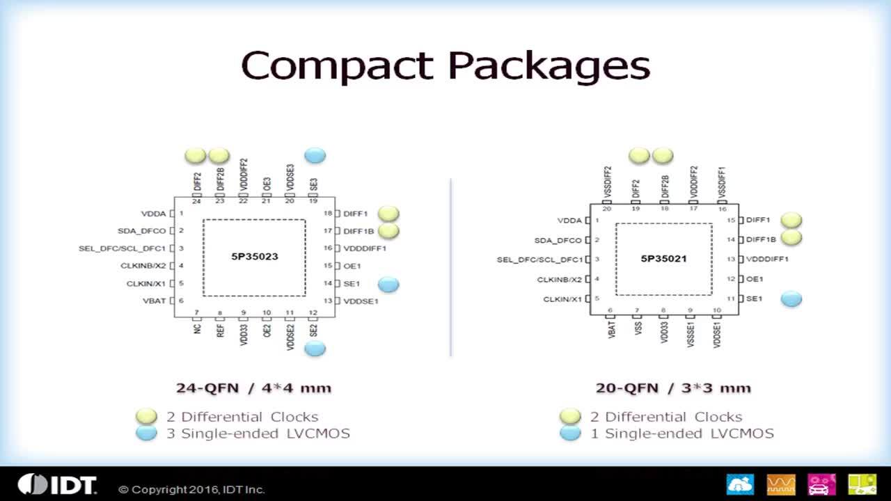
Package Options
| Pkg. Type | Pkg. Dimensions (mm) | Lead Count (#) | Pitch (mm) |
|---|---|---|---|
| VFQFPN | 4.0 x 4.0 x 0.9 | 24 | 0.5 |
Product Comparison
 | | | | |
| 5P35023 | 5P35021 | 5L35021 | 5L35023 | |
| Outputs (#) | 7 | 5 | 5 | 7 |
| Output Type | LP-HCSL, LVCMOS, LVDS, LVPECL | LP-HCSL, LVCMOS, LVDS, LVPECL | LP-HCSL, LVCMOS | LP-HCSL, LVCMOS |
| Core Voltage (V) | 3.3 | 3.3 | 1.8 | 1.8 |
| Output Voltage (V) | 1.8, 2.5, 3.3 | 1.8, 2.5, 3.3 | 1.8 | 1.8 |
| Pkg. Dimensions (mm) | 4.0 x 4.0 x 0.9 | 3.0 x 3.0 x 1.0 | 3.0 x 3.0 x 1.0 | 4.0 x 4.0 x 0.9 |
Application Block Diagrams
 | Pet Camera Robot Mobile pet camera robot with real-time video, audio, and wireless control. |
 | High-End Central Thermostat Central thermostat system integrates satellite thermostats for smart climate control and efficiency. |
 | Video Conferencing Camera with AI Capabilities AI-powered 360° video conferencing system with dual cameras and beamforming audio. |
 | High-End Feature-Rich HMI Platform Flexible HMI platform with rich feature support for display resolutions, audio, speakers, and more. |
 | Industrial Automation Platform with Arm Cortex-A53 This industrial automation platform is designed for Arm Cortex-A53 MPUs including the iMX8 series of application processors. |
 | Cost-Effective Digital Cluster with 4-channel AHL and Surround View Digital clusters boost safety by centralizing info and reducing costs with AHL and efficient PMICs. |
 | Battery-Powered Camera with AI Object Detection & Motion Sensing Battery-powered camera with AI for efficient motion detection, fast boot, and low-power object classification. |
 | Comprehensive ADAS & Autonomous Driving Hardware-Software System Complete hardware and software system for ADAS and automated driving including front camera, surround view, and LiDAR. |
 | Single Board Computer Gateway SBC gateway with Arm Cortex-A55 and Arm Cortex-M33 cores offers efficient processing, flexibility, and connectivity. |
 | Access Control System with NFC, Camera, and Capacitive Touch Authentication The access control system ensures security with NFC, Wi-Fi, PoE, local storage, and flexible OS support. |
 | Mobile Point of Sale (mPoS) Terminal Mobile PoS with secure, wireless, multi-payment support for seamless transactions anywhere. |
 | Vision AI Box A centralized control hub for managing multiple cameras and AI models. |
 | Vehicle Computer for Future E/E Architecture Next-generation vehicle computer system for advanced E/E architecture with high computing power. |
 | AI-Enabled Surveillance Camera AI-powered surveillance camera with DRP-AI boosts security with 4K imaging and low power. |
 | IoT Communications Gateway Hub Smart communication gateway syncs patient data with doctors via Bluetooth LE, NFC, and cloud connectivity. |
Complete Your Design
Explore complementary products to elevate your design
Renesas Boards & Kits

Evaluation Board Kit for RZ/G3E MPU
The RZ/G3E Evaluation Board Kit consists of a module board (SOM) and a carrier board, ideal for evaluating the features of the RZ/G3E MPU. The module board complies with the SMARC v2.1 standard and is a good reference for module board-based product development.
Main Contents:
- RZ/G3E SMARC Module... Read More
")
Vehicle Computer Generation 4
The VC4 is based on a complete Renesas chipset. The centerpiece is the R-Car S4 with 8x Cortex®A55 cores, 1x Cortex® R52 core 2x RH850 G4MH delivering up to 27K DMIPS application performance and up to 5.3K DMIPS lock step real-time performance. It incorporates an 8MB SRAM to execute code on the... Read More

RZ/A3UL Evaluation Board Kit
This evaluation board kit is ideal for evaluating RZ/A3UL. The RZ/A3UL Evaluation Board Kit consists of a module board (SOM) and a carrier board. The module board complies with the SMARC v2.1 standard.
Two types of evaluation boards are available: QSPI version and Octal-SPI version.
- QSPI version:... Read More

Evaluation Board Kit for RZ/Five MPU
The RZ/Five evaluation kit (EVK) is ideal for evaluating and developing with the Renesas RZ/Five MPU. The EVK includes the RZ/Five SMARC v2.1 System on Module (SoM) and its carrier board. The module board complies with the SMARC v2.1 standard.
- Contents
- RZ/Five (RISC-V) Module Board (SMARC2.1)

Evaluation Board Kit for RZ/G2UL MPU
This evaluation board kit is ideal for evaluating RZ/G2UL. The RZ/G2UL Evaluation Board Kit consists of a module board (SOM) and a carrier board. The module board complies with the SMARC v2.1 standard.
Contents:
- RZ/G2UL Module Board (SMARC2.1)
- Common Carrier Board (For RZ/G2L, RZ/G2LC, RZ/G2UL and... Read More

SMARC SOM Evaluation Kit for RZ/V2L MPU with AI Accelerator
The RZ/V2L Evaluation Board Kit consists of a module board (SOM) and a carrier board that can easily start evaluation of the RZ/V2L. It also includes the MIPI Camera Module (MIPI CSI). The carrier board can be commonly used with RZ/G2L, RZ/G2LC, RZ/G2UL, and RZ/V2L modules (SOM) prepared... Read More
Test This Board Remotely

Evaluation Board Kit for RZ/G2LC MPU
This evaluation board kit is ideal for evaluating RZ/G2LC. The RZ/G2LC Evaluation Board Kit consists of a module board (SOM) and a carrier board. The module board complies with the SMARC v2.1 standard.
- Contents
- RZ/G2LC Module Board (SMARC2.1)
- Common Carrier Board (For RZ/G2L, RZ/G2LC, RZ/G2UL and...

Evaluation Board Kit for RZ/G2L MPU
This evaluation board kit is ideal for evaluating RZ/G2L. The RZ/G2L Evaluation Board Kit consists of a module board (SOM) and a carrier board. The module board complies with the SMARC v2.1 standard.
- Contents
- RZ/G2L Module Board (SMARC2.1)
- Common Carrier Board (For RZ/G2L, RZ/G2LC, RZ/G2UL and...
Test This Board Remotely

ADAS & Automated Driving Solution R-Car V3H Development Board/Condor-I
The combination of the R-Car, the PMIC, and the clock generators provides a high-efficiency and high-end ADAS solution that supports image input, image output, and high-speed input/output IF.

5P35023 and 5X35023 VersaClock 3S Programmable Clock Development Kit
The DEV5P35023 programmable clock development kit is designed to support the 5P35023 and 5X35023 VersaClock 3S devices. It provides a convenient way of configuring and programming the blank parts for the 5P35023 and 5X35023 devices. With the onboard USB interface, the Renesas Timing CommanderTM... Read More

Programmer Board for VersaClock 3S - 5P3502x
The VersaClock® 3S-5P3502x programmer board is made to ease the programming of blank 5P35021 and 5P35023 devices. With the on-board USB interface, the Renesas Timing Commander™ graphical user interface (GUI) is used to communicate with the blank device in the socket for configuration and... Read More
Partner Boards & Kits
OSM-L System on Module (SoM) Powered by RZ/G2L

REGULUS RZ/V2L & RZ/G2L SMARC System on Module (SoM)
")
RZ/G2L SMARC 2.1 Compliant System-on-Module (SoM)

RZ/G2L SMARC System on Module (SoM)

RZ/G3E DX-M1 System on Module (SoM)

RZ/G3E OSM-L
RZ/G3E System on Module (SoM)
RZ/V2L SMARC 2.1 Compliant System-on-Module (SoM)
TRIA SM2S-G2L
TRIA SM2S-V2L

VK-CM-RZ/V2L

VK-RZ/G2LC

VK-RZ/V2L

RZ/V2L PerCV.AI Reference Design
Our RZ/V2L SoM offers a versatile platform packed with features and connectivity options like wireless, USB, and CAN, simplifying the integration of system components. Paired with the RZ/V2L SoM MXT AI board, we empower developers to jumpstart hardware and software development with robust tools... Read More
Test This Board Remotely
Support Communities
-
5P35023 not reacting to configuration changes
After power-up the (blank) 5P35023 DIFF1/2 outputs deliver 4x the crystal frequency, which is the default documented in the data sheet. In our case it's 40 MHz from a 10 MHz oscillator. I read back the initial register content via I2C, and it matches the data ...
Mar 1, 2026 -
5P35023, About POR electrical conditions
Hello specialist, Please let me know about the POR electrical characteristics of the 5P35023, following items. reset voltage threshold release voltage from reset condition REF clock behavior during reset(*)At what voltage does the reset occur within the device's recommended operating range of 3.135~3.3~3.465V ...
Dec 6, 2024 -
5V49EE702NDGI8 vs 5V49EE702-097NDGI8
Hello.Could you please help to clarify tech details of difference 5V49EE702NDGI8 vs 5V49EE702-097NDGI8.I know that suffix -097 refers to Optional Dash Number (attached document). But I need more deep datails because 5V49EE702-097NDGI8 doesn't work well when i soldered it as replacement of 5V49EE702NDGI8. Thank you ...
Feb 8, 2024
Knowledge Base
-
RZ family: RAA215300 and 5P35023B-629NLGI on RZ/G2L EVK
Last Updated: 09/24/2025 Question: When using the RZ/G2L evaluation board, are the PMIC and clock generator (e.g., RAA215300 and 5P35023B-629NLGI) pre-programmed with the necessary voltage and frequency settings, or do they need to be configured via I2C after the CPU starts ...
Sep 24, 2025 -
RZ/G2L, LC: Clock
5P35023B-629NLGI of VersaClock3S is used. EXTAL and audio clock and a clock for each of Ethernet PHY and audio DAC incorporated in the evaluation board are provided.
Oct 27, 2021 -
RZ/Five: Can you tell me what clock generator is used with the evaluation board for the RZ/Five?
Last Updated: 09/21/2022 Question: Can you tell me what clock generator is used with the evaluation board for the RZ/Five? Answer: 5P35023B-629NLGI of VersaClock3S is used. EXTAL and audio clock and a clock for each of Ethernet PHY and audio DAC incorporated in ...
Sep 21, 2022

Support Communities


