特長
- OE、PD#、PPS、DFCの制御機能としてOEピンの機能を設定可能
- PLL帯域幅の設定可能/ジッタピーキングの最小化
- PPS:エンドデバイスのパワーダウン・モード時に電力を節約するプロアクティブ省電力機能
- PPB:Performance- Power Balancing機能により、必要な性能に応じた最小限の電力消費を実現
- DFC:Dynamic Frequency Control機能により、最大4つの異なる周波数をダイナミックに切り替え可能
- スペクトラム拡散クロックに対応し、システムEMIの低減を実現
- I2Cインタフェース
- 水晶振動器の入力にも対応
- AEC-Q100準拠、グレード2(-40℃〜+105℃)バージョンで利用可能


説明
パラメータ
| 属性 | 値 |
|---|---|
| Diff. Outputs | 2 |
| App Jitter Compliance | PCIe Gen1, PCIe Gen2, PCIe Gen3 |
| Outputs (#) | 7 |
| Output Type | LVCMOS, LVPECL, LP-HCSL, LVDS |
| Output Freq Range (MHz) | 0.032768 - 500 |
| Input Freq (MHz) | 1 - 160 |
| Inputs (#) | 1 |
| Input Type | Crystal, LVCMOS, LVPECL, LVDS, LP-HCSL |
| Output Banks (#) | 5 |
| Core Voltage (V) | 3.3 |
| Output Voltage (V) | 1.8V, 2.5V, 3.3V |
| Product Category | VersaClock 3S, Automotive Timing, General Purpose Clocks, PCI Express Clocks, Programmable Clocks |
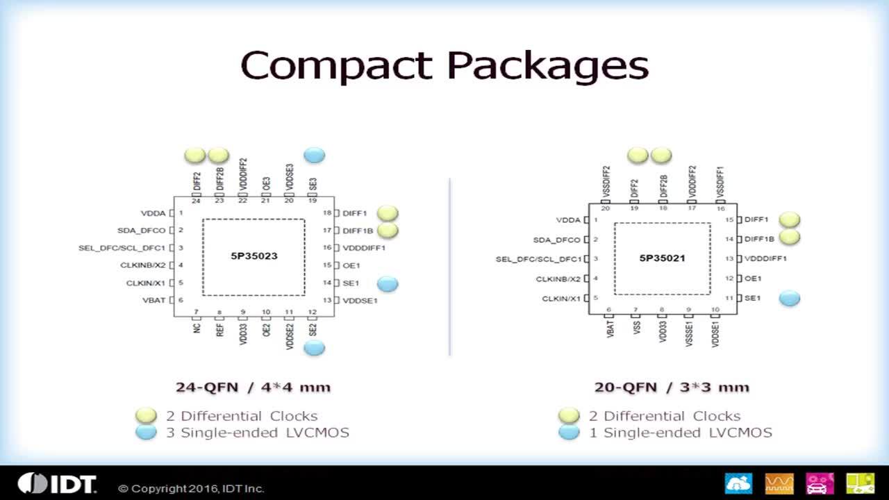
パッケージオプション
| Pkg. Type | Pkg. Dimensions (mm) | Lead Count (#) | Pitch (mm) |
|---|---|---|---|
| VFQFPN | 4.0 x 4.0 x 0.9 | 24 | 0.5 |
製品比較
| 5P35023 | 5P35021 | 5L35021 | 5L35023 | |
| Outputs (#) | 7 | 5 | 5 | 7 |
| Output Type | LP-HCSL, LVCMOS, LVDS, LVPECL | LP-HCSL, LVCMOS, LVDS, LVPECL | LP-HCSL, LVCMOS | LP-HCSL, LVCMOS |
| Core Voltage (V) | 3.3 | 3.3 | 1.8 | 1.8 |
| Output Voltage (V) | 1.8, 2.5, 3.3 | 1.8, 2.5, 3.3 | 1.8 | 1.8 |
| Pkg. Dimensions (mm) | 4.0 x 4.0 x 0.9 | 3.0 x 3.0 x 1.0 | 3.0 x 3.0 x 1.0 | 4.0 x 4.0 x 0.9 |
アプリケーション・ブロック図
 | ペット監視用カメラロボット リアルタイムの映像、音声、ワイヤレスコントロールが可能なモバイルペット監視用カメラロボット。 |
 | 高性能な集中制御式サーモスタットシステム 集中制御式サーモスタットシステムは、複数のサーモスタットを統合し、スマートな空調制御と効率化を実現します。 |
 | AI機能付きビデオ会議カメラ デュアルカメラとビームフォーミングオーディオを搭載したAI搭載360°ビデオ会議システム。 |
 | ハイエンドの機能豊富なHMIプラットフォーム ディスプレイ解像度、オーディオ、スピーカなどの豊富な機能をサポートする柔軟なHMIプラットフォーム。 |
 | シングルボードコンピュータゲートウェイ Arm Cortex-A55およびArm Cortex-M33コアを搭載したSBCゲートウェイは、効率的な処理、柔軟性、および接続性を提供します。 |
 | AI物体検出とモーションセンシングを備えたバッテリ駆動カメラ 効率的なモーション検出、高速起動、低電力のオブジェクト分類を実現するAI搭載のバッテリ駆動カメラ。 |
 | NFC、カメラ、静電容量式タッチ認証を備えたアクセス制御システム アクセス制御システムは、NFC、Wi-Fi、PoE、ローカルストレージ、および柔軟なOSサポートにより、セキュリティを確保します。 |
 | モバイルPOS(Point of Sale)端末 安全なワイヤレスのマルチペイメントをサポートするモバイルPOSで、どこでもシームレスな取引が可能です。 |
 | ビジョンAIゲートウェイ 複数のカメラとAIモデルを管理するための中央制御ハブ |
 | 将来のE/Eアーキテクチャのための車載コンピュータ 高度なE/Eアーキテクチャを高い計算能力で実現する次世代車載コンピュータシステム。 |
 | AI搭載モニタリングカメラ DRP-AIを搭載したAI搭載モニタリングカメラ、4K画像と低消費電力でセキュリティを強化します。 |
 | IoT 通信ゲートウェイ ハブ スマート通信ゲートウェイは、Bluetooth LE、NFC、およびクラウド接続を介して患者データを医師と同期します。 |
 | 高度なHMIおよびエッジAIアプリケーション向けのシングルボードコンピュータ Compact SBCは、デュアルコアMPU、DRP-AI、Wi-Fi、Bluetooth LE、NFC接続により、HMIとエッジAIをサポートします。 |
 | 4チャンネルAHLとサラウンドビューを備えた費用対効果の高いデジタルクラスタ デジタルクラスタは、AHLと効率的なPMICにより情報を一元化し、コストを削減することで安全性を高めます。 |
 | Arm Cortex-A53搭載の産業用オートメーションプラットフォーム この産業用オートメーションプラットフォームは、iMX8シリーズのアプリケーションプロセッサを含むArm Cortex-A53 MPU向けに設計されています。 |
このデバイスに組み合わせたい製品
更に設計開発を進めるための製品を探してみましょう
Renesas Boards & Kits

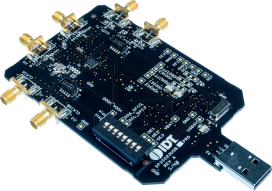
5P35023 and 5X35023 VersaClock 3S Programmable Clock Development Kit
The DEV5P35023 programmable clock development kit is designed to support the 5P35023 and 5X35023 VersaClock 3S devices. It provides a convenient way of configuring and programming the blank parts for the 5P35023 and 5X35023 devices. With the onboard USB interface, the Renesas Timing CommanderTM... 続きを読む
Programmer Board for VersaClock 3S - 5P3502x
The VersaClock® 3S-5P3502x programmer board is made to ease the programming of blank 5P35021 and 5P35023 devices. With the on-board USB interface, the Renesas Timing Commander™ graphical user interface (GUI) is used to communicate with the blank device in the socket for configuration and... 続きを読む

ADAS & Automated Driving ソリューション R-Car V3H 開発ボード / Condor-I
R-Car SoCとPMICをはじめとする各種電源ICとクロックジェネレータのコンビネーションにより、画像入力、画像出力や高速入出力IFに対応した高効率で高性能なADAS ソリューションを実現します。

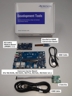
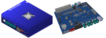
Evaluation Board Kit for RZ/G2L MPU
RZ/G2Lの評価に最適な評価ボードキットです。RZ/G2L Evaluation Board Kitはモジュールボード(SOM)とキャリアボードで構成されています。モジュールボードはSMARC v2.1規格に準拠しています。
- 同梱物
- RZ/G2L Module Board (SMARC2.1)
- Common Carrier Board (For RZ/G2L, RZ/G2LC, RZ/G2UL and RZ/V2L)
- USBケーブル(USB Type-A- Micro USB Type-B)
※以下はお客様で別途購入が必要なものです。
- USB type C 充電器 65W
- USB...
このボードをリモートでテストする

Evaluation Board Kit for RZ/G2LC MPU
RZ/G2LCの評価に最適な評価ボードキットです。RZ/G2LC Evaluation Board Kitはモジュールボード(SOM)とキャリアボードで構成されています。モジュールボードはSMARC v2.1規格に準拠しています。
- 同梱物
- RZ/G2LC Module Board (SMARC2.1)
- Common Carrier Board (For RZ/G2L, RZ/G2LC, RZ/G2UL and RZ/V2L)
- USBケーブル(USB Type-A- Micro USB Type-B)
※以下はお客様で別途購入が必要なものです。
- USB type C 充電器 65W
- USB...

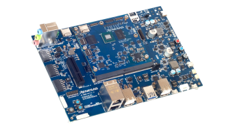
RZ/V2L Evaluation Board Kit
RZ/V2Lの評価に最適な評価ボードキットです。RZ/V2L Evaluation Board Kitはモジュールボード(SOM)とキャリアボードで構成されています。また、MIPIカメラモジュール(MIPI CSI)を同梱しています。キャリアボードはSMARC v2.1規格に沿って準備されるRZ/G2L、RZ/G2LC、RZ/G2UL、およびRZ/V2L用のモジュール(SOM)で共通に使用することができます。これにより、これらのデバイス間でシームレスかつフレキシブルな評価が体験できます。
このボードをリモートでテストする

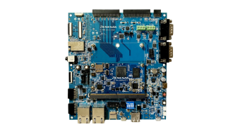
Evaluation Board Kit for RZ/G2UL MPU
RZ/G2ULの評価に最適な評価ボードキットです。RZ/G2UL Evaluation Board Kitはモジュールボード(SOM)とキャリアボードで構成されています。モジュールボードはSMARC v2.1規格に準拠しています。
同梱物:
- RZ/G2ULC Module Board (SMARC2.1)
- Common Carrier Board (For RZ/G2L, RZ/G2LC, RZ/G2UL and RZ/V2L)
- USBケーブル(USB Type-A Micro USB Type-B)
※以下はお客様で別途購入が必要なものです。
- USB type C 充電器 65W
- USB...
RZ/A3UL Evaluation Board Kit
RZ/A3ULの評価に最適な評価ボードキットです。RZ/A3UL Evaluation Board Kitはモジュールボード(SOM)とキャリアボードで構成されています。モジュールボードはSMARC v2.1規格に準拠しています。
なお、評価ボードはQSPI版とOctal-SPI版があります。
- QSPI版 :メモリ構成/ QSPI Serial Flash(Boot) + DDR4:RTK9763U02S01002BE
- Octal-SPI版 :メモリ構成/ Octa Flash(Boot) + OctaRAM + DDR4:RTK9763U02S01003BE
RZ/A3UL... 続きを読む
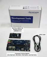
Evaluation Board Kit for RZ/Five MPU
Vehicle Computer Generation 4
The VC4 is based on a complete Renesas chipset. The centerpiece is the R-Car S4 with 8x Cortex®A55 cores, 1x Cortex® R52 core 2x RH850 G4MH delivering up to 27K DMIPS application performance and up to 5.3K DMIPS lock step real-time performance. It incorporates an 8MB SRAM to execute code on the... 続きを読む
Evaluation Board Kit for RZ/G3E MPU
RZ/G3E評価ボードキットは、モジュールボード(SOM)とキャリアボードで構成されており、RZ/G3E MPUの機能評価に最適です。モジュールボードはSMARC v2.1規格に準拠しており、モジュールボードベースの製品開発をご検討のユーザにとって優れたリファレンスとなります。
主な同梱物:
- RZ/G3E SMARC Module Board (SMARC2.1)
- Common Carrier Board II (For RZ/G3S and RZ/G3E)
- 各種アダプターボード、ケーブル、ネジ、他
※以下はお客様で別途購入が必要なものです。
- USB type C 充電器 65WとUSB type... 続きを読む
Partner Boards & Kits
OSM-L System on Module (SoM) Powered by RZ/G2L
REGULUS RZ/V2L & RZ/G2L SMARC System on Module (SoM)
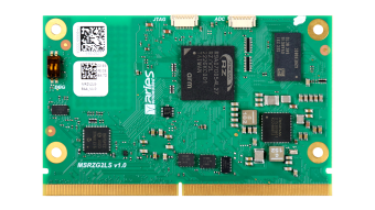
RZ/G2L SMARC 2.1 Compliant System on Module (SoM)
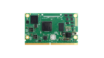
RZ/G2L SMARC System on Module (SoM)
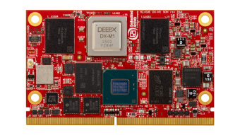
RZ/G3E DX-M1 System on Module (SoM)
RZ/G3E OSM-L
RZ/G3E System on Module (SoM)
RZ/V2L SMARC 2.1 Compliant System on Module (SoM)
TRIA SM2S-G2L
TRIA SM2S-V2L
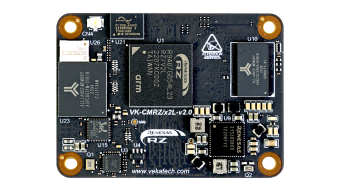
VK-CM-RZ/V2L
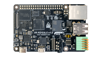
VK-RZ/G2LC
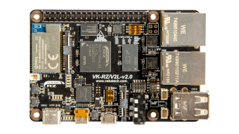
VK-RZ/V2L

RZ/V2L PerCV.AI Reference Design
Our RZ/V2L SoM offers a versatile platform packed with features and connectivity options like wireless, USB, and CAN, simplifying the integration of system components. Paired with the RZ/V2L SoM MXT AI board, we empower developers to jumpstart hardware and software development with robust tools... 続きを読む
