特長
- OE、PD#、PPS、DFCの制御機能としてOEピンの機能を設定可能
- PLL帯域幅の設定可能/ジッタピーキングの最小化
- PPS:エンドデバイスのパワーダウン・モード時に電力を節約するプロアクティブ省電力機能
- PPB:Performance- Power Balancing機能により、必要な性能に応じた最小限の電力消費を実現
- DFC:Dynamic Frequency Control機能により、最大4つの異なる周波数をダイナミックに切り替え可能
- スペクトラム拡散クロックに対応し、システムEMIの低減を実現
- I2Cインタフェース
-
水晶振動器の入力にも対応
-
AEC-Q100準拠、グレード2(-40℃〜+105℃)バージョンで利用可能
説明
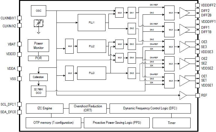
5P35023はVersaClock®プログラマブルクロックジェネレータで、低消費電力、消費者用、高性能 PCI Expressアプリケーション向けに設計されています。 5P35023は3つのPLLアーキテクチャ設計で、各PLLは個別にプログラム可能で、最大5つのユニークな周波数出力を可能にします。5P35023は、PPS(Proactive Power Saving)、PPB(Performance-Power Balancing)、ORT(Overshot Reduction Technology)、超低電力DCOなどのユニークな機能を内蔵しています。 OTPメモリを内蔵しているため、電源投入後にプログラミングをせずにデバイスに設定を保存し、その後I2Cインタフェースから再度5P35023をプログラミングすることが可能です。
5P35023はプログラマブルなVCOとPLLソースの選択により、アプリケーションの要件に基づいた電力性能の最適化を可能にします。 また、LVCMOS、LVPECL、LVDS、LPHCSLに対応した3つのシングルエンド出力と2組の差動出力に対応しています。 システムRTCのリファレンスクロックとして、消費電流5μA以下の32.768kHzのLow Powerクロックをサポートします。
製品比較
| 5P35023 | 5L35021 | 5L35023 | 5P35021 | |
| Outputs (#) | 7 | 5 | 7 | 5 |
| Output Type | LP-HCSL, LVCMOS, LVDS, LVPECL | LP-HCSL, LVCMOS | LP-HCSL, LVCMOS | LP-HCSL, LVCMOS, LVDS, LVPECL |
| Core Voltage (V) | 3.3 | 1.8 | 1.8 | 3.3 |
| Output Voltage (V) | 1.8, 2.5, 3.3 | 1.8 | 1.8 | 1.8, 2.5, 3.3 |
| Pkg. Dimensions (mm) | 4.0 x 4.0 x 0.9 | 3.0 x 3.0 x 1.0 | 4.0 x 4.0 x 0.9 | 3.0 x 3.0 x 1.0 |
パラメータ
| 属性 | 値 |
|---|---|
| App Jitter Compliance | PCIe Gen1, PCIe Gen2, PCIe Gen3 |
| Outputs (#) | 7 |
| Output Type | LVCMOS, LVPECL, LP-HCSL, LVDS |
| Output Freq Range (MHz) | - |
| Input Freq (MHz) | - |
| Inputs (#) | 1 |
| Input Type | Crystal, LVCMOS, LVPECL, LVDS, LP-HCSL |
| Output Banks (#) | 5 |
| Core Voltage (V) | 3.3 |
| Output Voltage (V) | 1.8, 2.5, 3.3 |
| Phase Jitter Typ RMS (ps) | 3 |
| Prog. Interface | I2C, OTP |
| Spread Spectrum | Yes |
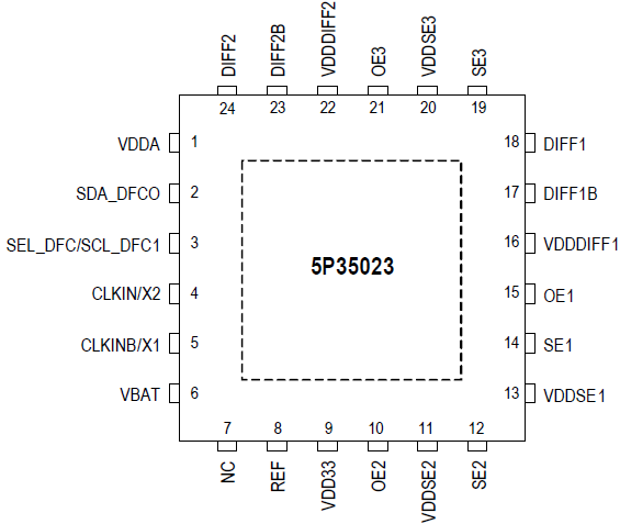
パッケージオプション
| Pkg. Type | Pkg. Dimensions (mm) | Lead Count (#) | Pitch (mm) |
|---|---|---|---|
| VFQFPN | 4.0 x 4.0 x 0.9 | 24 | 0.5 |
アプリケーション・ブロック図

|
AI機能付きビデオ会議カメラ
デュアルカメラとビームフォーミングオーディオを搭載したAI搭載360°ビデオ会議システム。
|

|
ハイエンドの機能豊富なHMIプラットフォーム
ディスプレイ解像度、オーディオ、スピーカなどの豊富な機能をサポートする柔軟なHMIプラットフォーム。
|

|
シングルボードコンピュータゲートウェイ
Arm Cortex-A55およびArm Cortex-M33コアを搭載したSBCゲートウェイは、効率的な処理、柔軟性、および接続性を提供します。
|

|
視覚物体検出 SoM
視覚検出SoMは、AI MPU、ワイヤレスIoT、およびスマート分析のための低コストのモジュラ設計を特長としています。
|

|
AI物体検出とモーションセンシングを備えたバッテリ駆動カメラ
効率的なモーション検出、高速起動、低電力のオブジェクト分類を実現するAI搭載のバッテリ駆動カメラ。
|

|
NFC、カメラ、静電容量式タッチ認証を備えたアクセス制御システム
アクセス制御システムは、NFC、Wi-Fi、PoE、ローカルストレージ、および柔軟なOSサポートにより、セキュリティを確保します。
|

|
コンピュータビジョン用システムオンモジュール(SoM)
ルネサスのSoMは、AI、コスト効率、シームレスなSMARC 2.1統合により、コンピュータビジョンを強化します。
|

|
モバイルPOS(Point of Sale)端末
安全なワイヤレスのマルチペイメントをサポートするモバイルPOSで、どこでもシームレスな取引が可能です。
|

|
MPUベースのシングルボードコンピュータ
Linuxサポート、ワイヤレス接続、組み込みアプリケーション向けのコンパクトなフォームファクタを備えたSBC。
|

|
Bluetooth Low Energyメッシュ用ネットワークゲートウェイ
デュアルコアMPU、Bluetooth LEメッシュ、Wi-Fi、ローカル/クラウドストレージ、アラーム、セキュア通信を備えたゲートウェイ設計。
|

|
RISC-V MPU を搭載したスケーラブルな SMARC 2.1 ゲートウェイ SoM
IIoTゲートウェイ向けのスケーラブルなSMARC 2.1 SoM設計は、低消費電力、強力な接続性、柔軟性を備えています。
|

|
RTOSベースのRZ/A3UL HMI SMARC SoM
スマートビルディングでの低電力およびリアルタイムHMI制御に最適化された電力を備えたSOM。
|

|
将来のE/Eアーキテクチャのための車載コンピュータ
高度なE/Eアーキテクチャを高い計算能力で実現する次世代車載コンピュータシステム。
|

|
シングルコアArm Cortex-A55 MPU用SMARCシステム
Arm Cortex-A55 MPUを搭載したAI対応SMARC SoMにより、低消費電力のHMIおよび産業用制御を実現します。
|

|
AI搭載モニタリングカメラ
DRP-AIを搭載したAI搭載モニタリングカメラ、4K画像と低消費電力でセキュリティを強化します。
|