Renesas Electronics Corporation - June is Pride Month, a month to raise awareness of the rights and the culture of the LGBTQ+ community

Features

  • Low skew, fanout buffer
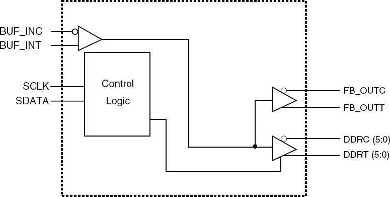
  • SMBus for functional and output control
  • Single bank 1-6 differential clock distribution
  • 1 pair of differential feedback pins for input to output synchronization
  • Supports up to 2 DDR DIMMs
  • 266MHz (DDRI 533) output frequency support
  • 400MHz (DDRII 800) output frequency support
  • Programmable skew through SMBus
  • Individual output control programmable through SMBus
  • OUTPUT - OUTPUT skew: <100ps
  • Output Rise and Fall Time for DDR outputs: 650ps - 950ps
  • DUTY CYCLE: 47% - 53%
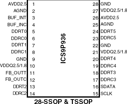
  • 28-pin SSOP/TSSOP package
  • RoHS compliant packaging

Description

Dual DDR I/II fanout buffer for VIA Chipset

Part NumberStatusSamplesStockPackageLead Count (#)Carrier TypeMoisture Sensitivity Level (MSL)Qty. per Reel (#)Qty. per Carrier (#)Package Area (mm²)Pkg. Dimensions (mm)Pb (Lead) FreePb Free CategoryTemp. Range (°C)
9P936AFLFObsoleteN/AIn StockSSOP28#Tube1047#54.1mm²10.2 x 5.3 x 1.73Yese3 Sn0 to 70°C
9P936AFLFTObsoleteN/AIn StockSSOP28#Reel11500#054.1mm²10.2 x 5.3 x 1.73Yese3 Sn0 to 70°C
9P936AGLFObsoleteN/AOut of StockTSSOP28#Tube1050#42.7mm²9.7 x 4.4 x 1.0Yese3 Sn0 to 70°C
9P936AGLFTObsoleteN/AOut of StockTSSOP28#Reel12000#042.7mm²9.7 x 4.4 x 1.0Yese3 Sn0 to 70°C
Support Communities

Support Communities

Get quick technical support online from Renesas Engineering Community technical staff.
Browse Articles

Knowledge Base

Browse our knowledge base for helpful articles, FAQs, and other useful resources.
Submit a Ticket

Submit a Ticket

Need to ask a technical question or share confidential information?