
Features
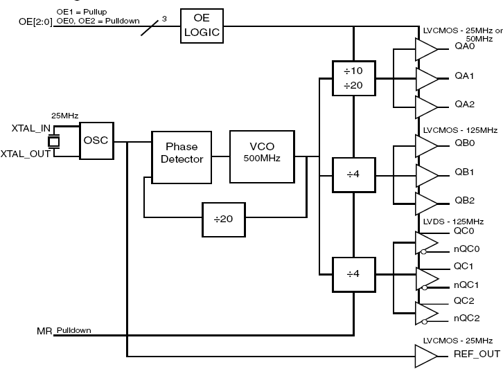
- Three banks of outputs: Bank A: three single-ended LVCMOS/LVTTL outputs at 25MHz or 50MHz Bank B: three single-ended LVCMOS/LVTTL outputs at 125MHz Bank C: three differential LVDS outputs at 125MHz Reference LVCMOS/LVTTL output at 25MHz
- Crystal input frequency: 25MHz
- Maximum output frequency: 125MHz
- RMS phase jitter @ 125MHz, using a 25MHz crystal (637kHz - 62.5MHz): 0.373ps (typical) LVDS output
- RMS phase jitter @ 25MHz, using a 25MHz crystal (12kHz - 1MHz): 0.64ps (typical) LVCMOS output
- Full 3.3V supply mode
- -40°C to 85°C ambient operating temperature
- Available in lead-free (RoHS 6) package
Description
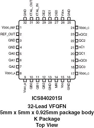
8402015I is a low phase noise clock synthesizer that provides three banks of outputs and a reference clock. Each bank can be enabled by using output enable pins. A 25MHz or 50MHz, 18pF parallel resonant crystal is used to generate 25MHz LVCMOS, 125MHz LVCMOS and 125MHz LVDS outputs. 8402015I is packaged in a small, 32-pin VFQFN package that is optimum for applications with space limitations.