特長
- PCIe Gen1-4準拠
- 終端の内蔵により100Ωの差動Zoを実現:部品点数と基板面積を削減
- 1.8V動作:消費電力の低減
- OE#端子:DIFパワーマネージメント対応
- LP-HCSL差動クロック出力:消費電力と基板面積の削減
- 各出力のプログラマブルスルーレート:様々な線長に対応したチューニングが可能
- プログラマブル出力振幅:様々なアプリケーション環境に対応したチューニングが可能
- PLLがロックされるまでのDIF出力ブロック:クリーンシステムスタートアップ
- 0%、-0.25%、-0.5%から選択可能なDIF出力スプレッド:EMIの低減
- 外付け25MHz水晶振動子、0ppmの合成エラーでタイトなppmをサポート
- ストラップピンによるコンフィギュレーションが可能:デバイス制御のためのSMBusインターフェースは不要
- レガシーコントローラ対応3.3V SMBusインタフェース
- 省スペース4x4mm 24ピンVFQFPN、最小限の基板スペースを実現

9FGV0241 - Block Diagram
説明
9FGV0241は、PCIe Gen1-4 アプリケーション向けの2出力超低電力周波数ジェネレータで、Zo=100 Ωの出力終端を内蔵しています。 クロック管理用に2つの出力イネーブルを備え、スペクトラム拡散オフに加えて、2種類のスペクトラム拡散レベルをサポートします。
パラメータ
| 属性 | 値 |
|---|---|
| Diff. Outputs | 2 |
| Diff. Output Signaling | LP-HCSL |
| Output Freq Range (MHz) | 25 - 25, 100 - 100 |
| Power Consumption Typ (mW) | 45 |
| Supply Voltage (V) | 1.8 - 1.8 |
| Output Type | LP-HCSL, LVCMOS |
| Xtal Freq (MHz) | 25 - 25 |
| Diff. Termination Resistors | 0 |
| Package Area (mm²) | 16 |
| Battery Backup | No |
| Battery Seal | No |
| CPU Supervisory Function POR | No |
| Crystal Frequency Trimming | No |
| Frequency Out Pin | No |
| Inputs (#) | 1 |
| Input Freq (MHz) | 25 - 25 |
| Function | Generator |
| Input Type | Crystal, LVCMOS |
| Core Voltage (V) | 1.8 |
| Output Voltage (V) | 0.8V, 1.8V |
| Product Category | PCI Express Clocks |
パッケージオプション
| Pkg. Type | Pkg. Dimensions (mm) | Lead Count (#) | Pitch (mm) |
|---|---|---|---|
| VFQFPN | 4.0 x 4.0 x 0.9 | 24 | 0.5 |
アプリケーション・ブロック図
 | 自動光学検査(AOI) DRP-AIおよびWi-Fi 6をサポートする強力なMPUにより、高速で低遅延のAOIシステムを実現します。 |
 | 複数のPHYを搭載したスマートホームコントローラ マルチスタンダードPHY、直感的なコントロール、将来を見据えた設計を備えたオールインワンスマートホームゲートウェイ。 |
 | Arm Cortex-A53搭載の産業用オートメーションプラットフォーム この産業用オートメーションプラットフォームは、iMX8シリーズのアプリケーションプロセッサを含むArm Cortex-A53 MPU向けに設計されています。 |
 | 高性能ヒューマンマシンインタフェース(HMI)システム 幅広いヒューマンマシンインタフェース機能を駆動するための汎用性の高いシステムオンモジュール(SoM)。 |
このデバイスに組み合わせたい製品
更に設計開発を進めるための製品を探してみましょう
RZ/G2UL
1.0GHz SingleコアArm Cortex-A55 CPU、200MHz SingleコアArm Cortex-M33 CPU、ギガビットイーサーネット2chなどを搭載の汎用マイクロプロセッサ
データシート
| 型名 | 状態 | サンプル | 長期供給 | 在庫 | パッケージ | 参考価格(米ドル) | Lead Count (#) | Carrier Type | Moisture Sensitivity Level (MSL) | Qty. per Reel (#) | Qty. per Carrier (#) | Pb (Lead) Free | Pb Free Category | Temp. Range (°C) | Country of Assembly | Country of Wafer Fabrication |
|---|---|---|---|---|---|---|---|---|---|---|---|---|---|---|---|---|
| 9FGV0241AKILF | Active | Available | 2040 Apr | 在庫あり | VFQFPN | 1ku | $1.21 | 24# | Tray | 1 | 0 | 490# | Yes | e3 Sn | -40 to 85°C | TAIWAN | TAIWAN |
| 9FGV0241AKILFT | Active | N/A | 2040 Apr | 在庫あり | VFQFPN | 1ku | $1.21 | 24# | Reel | 1 | 2500# | 0 | Yes | e3 Sn | -40 to 85°C | TAIWAN | TAIWAN |
| 9FGV0241AKLF | Active | Available | 2040 Apr | 在庫あり | VFQFPN | 1ku | $1.1 | 24# | Tray | 1 | 0 | 490# | Yes | e3 Sn | 0 to 70°C | TAIWAN | TAIWAN |
| 9FGV0241AKLFT | Active | N/A | 2040 Apr | 在庫あり | VFQFPN | 1ku | $1.1 | 24# | Reel | 1 | 2500# | 0 | Yes | e3 Sn | 0 to 70°C | TAIWAN | TAIWAN |
このデバイスに組み合わせたい製品
更に設計開発を進めるための製品を探してみましょう
RZ/G2UL
1.0GHz SingleコアArm Cortex-A55 CPU、200MHz SingleコアArm Cortex-M33 CPU、ギガビットイーサーネット2chなどを搭載の汎用マイクロプロセッサ
データシート
読込中
ログイン後、ご登録が可能となります。
- アプリケーションノート英語PDF 431 KB 7WDXRDKU4E7E-5-59216 2023年12月06日
- 製品変更通知英語PDF 734 KB 2022年11月16日
- 製品変更通知英語PDF 726 KB 2021年8月20日
- 製品変更通知英語PDF 5.71 MB 2020年6月09日
- アプリケーションノート英語PDF 307 KB 7WDXRDKU4E7E-5-59989 2016年3月10日
- アプリケーションノート英語PDF 1.9 MB 7WDXRDKU4E7E-5-57315 2014年5月13日
- アプリケーションノート英語PDF 495 KB 7WDXRDKU4E7E-5-57312 2014年5月12日
- アプリケーションノート英語PDF 442 KB 7WDXRDKU4E7E-5-57298 2014年5月08日
推奨ドキュメント (1)
データシート (1)
マニュアル、ガイド (1)
- アプリケーションノート英語PDF 431 KB 7WDXRDKU4E7E-5-59216 2023年12月06日
- アプリケーションノート英語PDF 1.99 MB 7WDXRDKU4E7E-5-57242 2022年3月01日
- アプリケーションノート英語PDF 307 KB 7WDXRDKU4E7E-5-59989 2016年3月10日もっと見る (14)
アプリケーションノート、ホワイトペーパー (14)
- 製品変更通知英語PDF 734 KB 2022年11月16日
- 製品変更通知英語PDF 726 KB 2021年8月20日
- 製品変更通知英語PDF 5.71 MB 2020年6月09日もっと見る (9)
製品通知(PCN、EOLなど) (9)
No Results Found.
キーワードを見直してみましょう。
入力するワードを減らしてみたり、異なるワード、あるいはより一般的なワードを入力してみましょう。
入力するワードを減らしてみたり、異なるワード、あるいはより一般的なワードを入力してみましょう。
フィルターを確認してみましょう。
フィルターを適用している場合、フィルターの範囲を見直してみてより広く検索結果が反映される様にしてみましょう。
フィルターを適用している場合、フィルターの範囲を見直してみてより広く検索結果が反映される様にしてみましょう。
お困りの場合は
- ナレッジベースを検索してみましょう。FAQにより、お客様をサポートいたします。
- ルネサスの技術スタッフやコミュニティからのヘルプをサポートフォーラムから受けられます。
図、設計ファイル (1)
No Results Found.
キーワードを見直してみましょう。
入力するワードを減らしてみたり、異なるワード、あるいはより一般的なワードを入力してみましょう。
入力するワードを減らしてみたり、異なるワード、あるいはより一般的なワードを入力してみましょう。
フィルターを確認してみましょう。
フィルターを適用している場合、フィルターの範囲を見直してみてより広く検索結果が反映される様にしてみましょう。
フィルターを適用している場合、フィルターの範囲を見直してみてより広く検索結果が反映される様にしてみましょう。
お困りの場合は
- ナレッジベースを検索してみましょう。FAQにより、お客様をサポートいたします。
- ルネサスの技術スタッフやコミュニティからのヘルプをサポートフォーラムから受けられます。
Renesas Boards & Kits
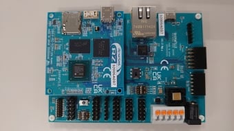
RZ/V2MA-EVKIT
アクティブ
RZ/V2MA Evaluation Board Kit
RZ/V2MAの評価に最適な評価ボードキットです。RZ/V2MA Evaluation Board Kitは、MainボードとBaseボード、 Optionボード(別売)で構成されています。OptionボードはPCIeインタフェースの評価に使用します。
本評価キットはRZ/V2MAの標準ソフトウェアパッケージに対応しており、低消費電力AI推論、Video Streaming等の機能を評価することが可能です。
プロバイダ:
シマフジ電機株式会社Partner Boards & Kits
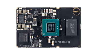
SoM/SBC
V2N System on Module (SoM)
Provides a cost‑effective embedded module powered by the Renesas RZ/V2N processor for AI‑driven vision applications. It supports two four‑lane MIPI CSI‑2 connections, enabling concurrent attachment of up to four cameras. Customization options include onboard Wi‑Fi® and Bluetooth®, configurable memory and storage capacities, and flexible physical layer settings. The module delivers a compact form factor, enhanced security features, and an integrated hardware and software solution supporting modular system design.
Provided By:
IMDT読込中
フィルター
適用されたフィルター
ソフトウェア/ツール
タイプでの検索
プロバイダでの検索
サンプルコード
アプリケーションでの検索
ファンクションでの検索
コンパイラでの検索
IDE に関するフィルタリング
シミュレーションモデル
Partner Solutions
No Results Found.
キーワードを見直してみましょう。
入力するワードを減らしてみたり、異なるワード、あるいはより一般的なワードを入力してみましょう。
入力するワードを減らしてみたり、異なるワード、あるいはより一般的なワードを入力してみましょう。
フィルターを確認してみましょう。
フィルターを適用している場合、フィルターの範囲を見直してみてより広く検索結果が反映される様にしてみましょう。
フィルターを適用している場合、フィルターの範囲を見直してみてより広く検索結果が反映される様にしてみましょう。
お困りの場合は
- ナレッジベースを検索してみましょう。FAQにより、お客様をサポートいたします。
- ルネサスの技術スタッフやコミュニティからのヘルプをサポートフォーラムから受けられます。
ソフトウェア/ツール (1)
No Results Found.
キーワードを見直してみましょう。
入力するワードを減らしてみたり、異なるワード、あるいはより一般的なワードを入力してみましょう。
入力するワードを減らしてみたり、異なるワード、あるいはより一般的なワードを入力してみましょう。
フィルターを確認してみましょう。
フィルターを適用している場合、フィルターの範囲を見直してみてより広く検索結果が反映される様にしてみましょう。
フィルターを適用している場合、フィルターの範囲を見直してみてより広く検索結果が反映される様にしてみましょう。
お困りの場合は
- ナレッジベースを検索してみましょう。FAQにより、お客様をサポートいたします。
- ルネサスの技術スタッフやコミュニティからのヘルプをサポートフォーラムから受けられます。
シミュレーションモデル (1)
No Results Found.
キーワードを見直してみましょう。
入力するワードを減らしてみたり、異なるワード、あるいはより一般的なワードを入力してみましょう。
入力するワードを減らしてみたり、異なるワード、あるいはより一般的なワードを入力してみましょう。
フィルターを確認してみましょう。
フィルターを適用している場合、フィルターの範囲を見直してみてより広く検索結果が反映される様にしてみましょう。
フィルターを適用している場合、フィルターの範囲を見直してみてより広く検索結果が反映される様にしてみましょう。
お困りの場合は
- ナレッジベースを検索してみましょう。FAQにより、お客様をサポートいたします。
- ルネサスの技術スタッフやコミュニティからのヘルプをサポートフォーラムから受けられます。
