
特長
- Accepts input frequencies ranging from 1PPS (1Hz) to 700MHz (1GHz in 3.3V HCSL mode)
- Two differential inputs support LVPECL, LVDS, LVHSTL, HCSL, or LVCMOS reference clocks
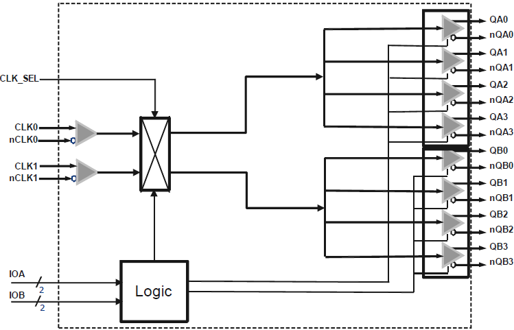
- Generates 8 differential or 16 LVCMOS outputs
- Outputs are arranged in two banks of four outputs each
- Select pins control which input drives which of the two output banks
- Controlled by 3-level input pins that are 3.3V-tolerant for all core voltages
- Output type may be selected from LVPECL, LVDS, HCSL, or CML
- Each bank supports a separate power supply of 3.3V, 2.5V, or 1.8V
- CML outputs support two different voltage swings
- Individual output enables and output type selection supported
- Output noise floor of –153dBc/Hz at 156.25MHz
- Core voltage supply of 3.3V, 2.5V, or 1.8V
- -40 °C to +85 °C ambient operating temperature
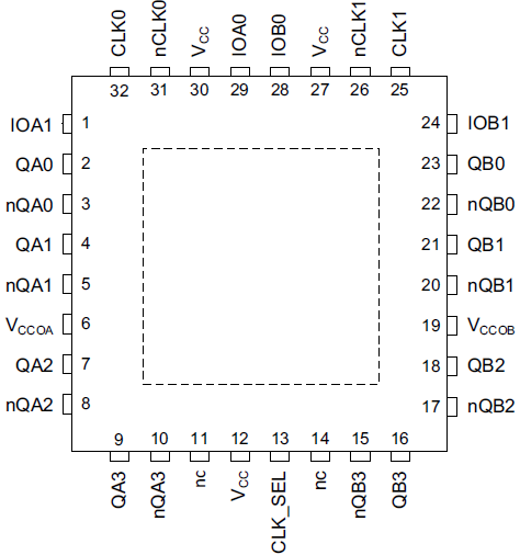
- Lead-free (RoHS 6) QFN-32 (5mm x 5mm) packaging
説明
The 8P391208 low additive jitter 2:8 buffer is intended to take one or two reference clocks, select between them using a pin selection, and generate up to eight outputs that are the same as the reference frequency. The 8P391208 supports two output banks, each with its own power supply. All outputs in one bank would generate the same output frequency, and each bank can be individually controlled for output type or output enable. The device can operate over the -40 °C to +85 °C temperature range.
パラメータ
| 属性 | 値 |
|---|---|
| Temp. Range (°C) | -40 to 85°C |
| Product Category | Clock Buffers & Drivers, RF Buffers |
パッケージオプション
| Pkg. Type | Pkg. Dimensions (mm) | Lead Count (#) | Pitch (mm) |
|---|---|---|---|
| VFQFPN | 5.0 x 5.0 x 0.9 | 32 | 0.5 |