
Features
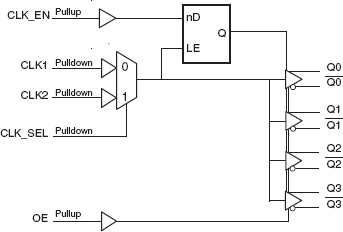
- Four differential LVDS output pairs
- Two LVCMOS/LVTTL clock inputs to support redundant or selectable frequency fanout applications
- Maximum output frequency: 650MHz
- Translates LVCMOS/LVTTL input signals to LVDS levels
- Output skew: 40ps (maximum)
- Part-to-part skew: 500ps (maximum)
- Propagation delay: 3.6ns (maximum)
- Additive phase jitter, RMS: 0.13ps (typical)
- Full 3.3Vsupply mode
- -40°C to 85°C ambient operating temperature
- Available in lead-free (RoHS 6) package
Description
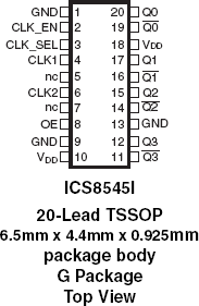
The 8545I is a low skew, high performance 1-to-4 LVCMOS/LVTTL-to-LVDS Clock Fanout Buffer and a member of the family of High Performance Clock Solutions from IDT. Utilizing Low Voltage Differential Signaling (LVDS) the 8545I provides a low power, low noise, solution for distributing clock signals over controlled impedances of 100?. The 8545I accepts a LVCMOS/LVTTL input level and translates it to 3.3V LVDS output levels. Guaranteed output and part-to-part skew characteristics make the 8545I ideal for those applications demanding well defined performance and repeatability.