
Features
- 15 - 0.7V current mode differential HSCL output pairs
- Pin compatible to 9EX21501/ Easy PCIe Gen3 upgrade
- 4 Selectable SMBus Addresses/Multiple devices can share the same SMBus Segment
- 8 dedicated and 2 group OE# pins/Hardware control of the outputs
- PLL or bypass mode/PLL can dejitter incoming clock
- Selectable PLL bandwidth/minimizes jitter peaking in downstream PLL's
- Spread Spectrum Compatible/tracks spreading input clock for low EMI
- SMBus Interface/unused outputs can be disabled
- Undriven differential outputs in Power Down mode/ Easy power management
- Cycle-to-cycle jitter <50ps
- Output-to-output skew < 150 ps
- PCIe Gen3 phase jitter < 1.0ps RMS
Description
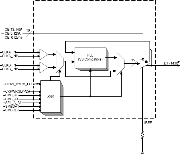
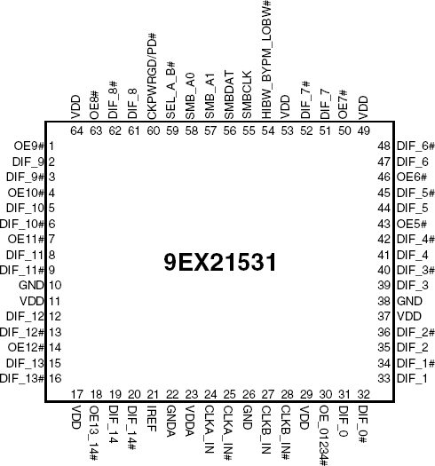
The 9EX21531 provides 15 output clocks for PCIe Gen1/ 2/3 applications. The 9EX21531 has 4 selectable SMBus addresses, and dedicated CKPWRGD/PD# and VDDA pins for easy board design. A differential clock from a CK410B+ or CK420BQ main clock generator, such as the 932S421, drives the 9EX21531. In fanout mode, the 9EX21531 provides outputs up to 166MHz.