
Features
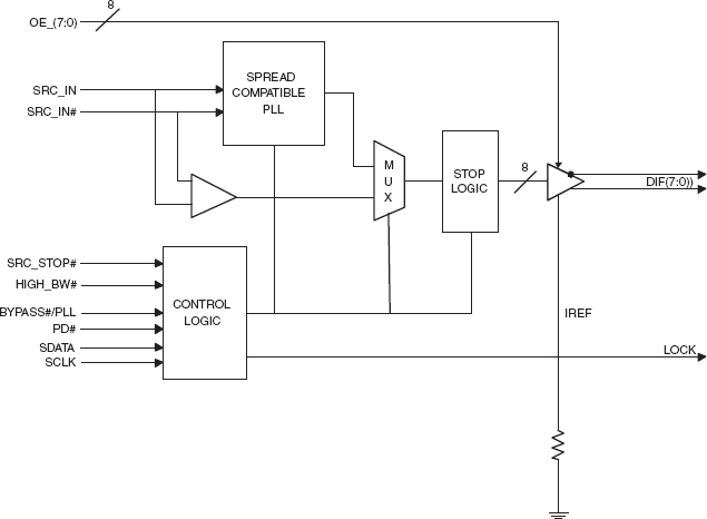
- 8 - 0.7 V current-mode differential output pairs
- Supports zero delay buffer mode and fanout mode
- Bandwidth programming available
- 50-100 MHz operation in PLL mode
- 50-400 MHz operation in Bypass mode
- Spread spectrum modulation tolerant, 0 to -0.5% down spread and +/- 0.25% center spread.
- Supports undriven differential outputs in PD# and SRC_STOP# modes for power management.
- Outputs cycle-cycle jitter < 50 ps
- Outputs skew: 50 ps
- Phase jitter: PCIe Gen1 < 86 ps peak to peak
- Phase jitter: PCIe Gen2 < 3.0/3.1 ps rms
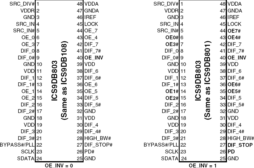
- 48-pin SSOP/TSSOP package
- RoHS compliant packaging
Description
The 9DB803 is compatible with the Intel DB800v2 Differential Buffer Specification. This buffer provides 8 PCI Express Gen2 clocks. The 9DB803 is driven by a differential output pair from a CK410B+, CK505 or CK509B main clock generator.
Parameters
| Attributes | Value |
|---|---|
| Diff. Outputs | 8 |
| Diff. Output Signaling | HCSL |
| Output Freq Range (MHz) | 33.33 - 400 |
| Diff. Inputs | 1 |
| Diff. Input Signaling | HCSL |
| Accepts Spread Spec Input | Yes |
| Power Consumption Typ (mW) | 578, 627 |
| Supply Voltage (V) | 3.3 - 3.3 |
| Output Type | HCSL |
| Diff. Termination Resistors | 32 |
| Package Area (mm²) | 76.3, 119.3 |
| Battery Backup | No |
| Battery Seal | No |
| CPU Supervisory Function POR | No |
| Crystal Frequency Trimming | No |
| Frequency Out Pin | No |
| Inputs (#) | 1 |
| Input Freq (MHz) | 100 |
| Function | Zero Delay Buffer |
| Input Type | HCSL |
| Output Banks (#) | 1 |
| Core Voltage (V) | 3.3 |
| Output Voltage (V) | 0.8 |
| Product Category | PCI Express Clocks |