
Features
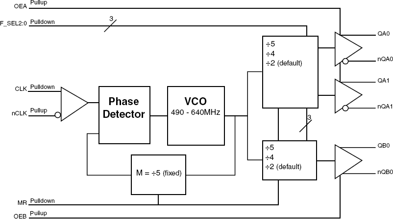
- Three differential LVDS output pairs
- One differential clock input
- CLK/nCLK can accept the following differential input levels: LVPECL, LVDS, LVHSTL, HCSL, SSTL
- Input frequency range: 98MHz to 128MHz
- Output frequency range: 98MHz to 320MHz
- VCO range: 490MHz - 640MHz
- Supports PCI Express® Spread-Spectrum Clocking
- High PLL bandwidth allows for better input tracking
- PCI Express® (2.5 Gb/s) and Gen 2 (5 Gb/S) jitter compliant
- 0°C to 70°C ambient operating temperature
- Full 3.3V operating supply
- Available in lead-free (RoHS 6) packages
Description
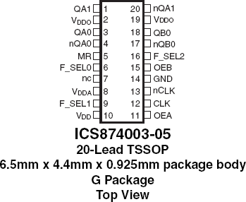
The 874003-05 is a high performance Differential-to-LVDS Jitter Attenuator designed for use in PCI Express® systems. In some PCI Express® systems, such as those found in desktop PCs, the PCI Express® clocks are generated from a low bandwidth, high phase noise PLL frequency synthesizer. In these systems, a jitter attenuator may be required to attenuate high frequency random and deterministic jitter components from the PLL synthesizer and from the system board. The 874003-05 has a bandwidth of 6.2MHz with <1dB peaking, easily meeting PCI Express® Gen2 PLL requirements. The 874003-05 uses IDT's 3rd Generation FemtoClock® PLL technology to achieve the lowest possible phase noise. The device is packaged in a 20 Lead TSSOP package, making it ideal for use in space constrained applications such as PCI Express® add-in cards.