
Features
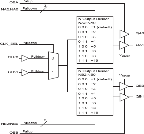
- Two banks of two LVCMOS/LVTTL outputs
- Selectable LVCMOS/LVTTL clock inputs
- LVCMOS_CLK supports the following input types: LVCMOS, LVTTL
- Maximum output frequency: 250MHz
- Output skew: 40ps (typical)
- Bank skew: 20ps (typical)
- Part-to-part skew: 60ps (typical)
- Power supply modes: CORE / OUTPUT 3.3V / 3.3V 3.3V / 2.5V 3.3V / 1.8V 2.5V / 2.5V 2.5V / 1.8V
- -40°C to 85°C ambient operating temperature
- Available in lead-free (RoHS 6) package
Description
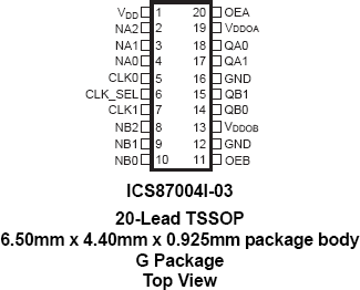
The 87004I-03 is a low skew, ÷1, ÷2 ÷3, ÷4 ÷5, ÷6 ÷8, ÷16 LVCMOS/LVTTL Fanout Buffer/Divider. The 87004I-03 has selectable clock inputs that accept single ended input levels. Output enable pin controls whether the output is in the active or high impedance state. The 87004I-03 is characterized at 3.3V, 2.5V and mixed 3.3V,2.5V, 3.3V,1.8V, 2.5V,1.8V input/output supply operating modes.Guaranteed bank, output, and part-to-part skew characteristics make the 87004I-03 ideal for those applications demanding well defined performance and repeatability.