
Features
- Three differential LVDS output pairs
- Three differential LVPECL clock input pairs
- PCLKx pair can accept the following differential input levels: LVPECL and LVDS
- Maximum output frequency: 2.5GHz
- Additive phase jitter, RMS: 0.035ps (typical)
- Propagation delay: 450ps (maximum)
- Part-to-part skew: 200ps (maximum)
- Full 2.5V supply mode
- -40°C to 85°C ambient operating temperature
- Available in lead-free (RoHS 6) package
Description
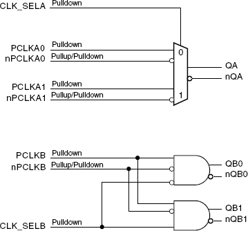
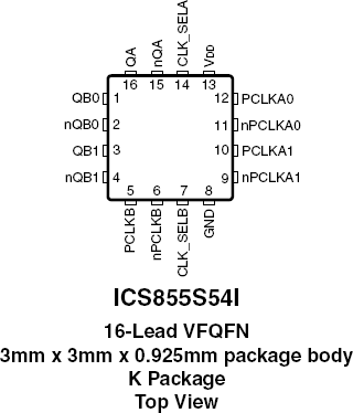
The 855S54I is a dual 2:1 and 1:2 Multiplexer. The 2:1 Multiplexer allows one of 2 inputs to be selected onto one output pin and the 1:2 MUX switches one input to one of two outputs. This device is useful for multiplexing multi-rate Ethernet PHYs which have 100 Mbit and 1 Gbit transmit/receive pairs onto an optical SFP module which has a single transmit/receive pair. See Application Section for further information. The 855S54I is optimized for applications requiring very high performance and has a maximum operating frequency of 2.5GHz. The device is packaged in a small, 3mm x 3mm VFQFN package, making it ideal for use on space-constrained boards.