
Features
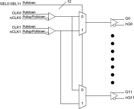
- Twelve, 2-to-1 multiplexers with LVPECL outputs
- Selectable differential CLKx, nCLKx input pairs
- CLK, nCLK pair can accept the following differential input levels: LVPECL, LVDS, LVHSTL, HCSL, SSTL
- Maximum output frequency: 700MHz
- Individual select control for each multiplexer
- Select inputs accept LVCMOS / LVTTL levels
- Propagation delay: 2ns (maximum)
- Additive Phase Jitter, RMS: 0.21ps (typical), 3.3V
- Full 3.3V or mixed 3.3V core/2.5V output supply
- -40°C to 85°C ambient operating temperature
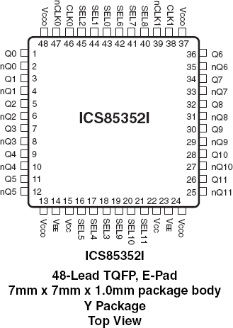
- Available in lead-free (RoHS 6) package
Description
The 85352I is a 12 bit, 2-to-1 LVPECL Clock Buffer. Individual input select controls support independent multiplexer operation from a common clock input source. Clock inputs accept most standard differential levels. The 85352I is characterized at full 3.3V or mixed 3.3V core/2.5V output operating supply modes.