
Features
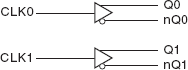
- Two differential 2.5V/3.3V LVPECL outputs
- Selectable CLK0, CLK1 LVCMOS/LVTTL clock inputs
- CLK0 and CLK1 can accepts the following input levels: LVCMOS or LVTTL
- Maximum output frequency: 267MHz
- Part-to-part skew: 250ps (maximum)
- 3.3V operating supply voltage (operating range 3.135V to 3.465V)
- 2.5V operating supply voltage (operating range 2.375V to 2.625V)
- -40°C to 85°C ambient operating temperature
- Available in standard (RoHS 5) or lead-free (RoHS 6) packages
Description
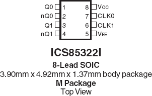
The 85322I is a Dual LVCMOS / LVTTL-to- Differential 2.5V / 3.3V LVPECL translator. The 85322I has selectable single ended clock inputs. The single ended clock input accepts LVCMOS or LVTTL input levels and translate them to 2.5V / 3.3V LVPECL levels. The small outline 8-pin SOIC package makes this device ideal for applications where space, high performance and low power are important.