
Features
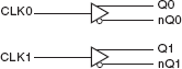
- 2 differential LVHSTL outputs
- Selectable CLK0, CLK1 LVCMOS clock inputs
- CLK0 and CLK1 can accept the following input levels: LVCMOS or LVTTL
- Maximum output frequency: 350MHz
- Part-to-part skew: 350ps (maximum)
- Propagation delay: 1.3ns (maximum)
- VOH: 1.2V (maximum)
- 3.3V and 2.5V operating supply
- 0°C to 70°C ambient operating temperature
- Industrial temperature information available upon request
- Lead-Free package fully RoHS compliant

Description
The 85222 is a Dual LVCMOS / LVTTL-to- Differential LVHSTL Translator. The 85222 has two single ended clock inputs. The single ended clock input accepts LVCMOS or LVTTL input levels and translates them to LVHSTL levels. The small outline 8-pin SOIC package makes this device ideal for applications where space, high performance and low power are important. For optimum performance, both output pairs need to be terminated, even if one output pair is unused.