
Features
- Four 0.7V differential HCSL outputs
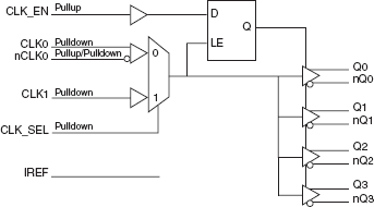
- Selectable differential CLK0, nCLK0 or LVCMOS inputs
- CLK0, nCLK0 pair can accept the following differential input levels: LVPECL, LVDS, LVHSTL, HCSL
- CLK1 can accept the following input levels: LVCMOS or LVTTL
- Maximum output frequency: 500MHz
- Translates any single-ended input signal to 3.3V HCSL levels with resistor bias on nCLK input
- Output skew: 100ps (maximum)
- Part-to-part skew: 600ps (maximum)
- Propagation delay: 3.2ns (maximum)
- Additive phase jitter, RMS: 0.22ps (typical)
- 3.3V operating supply
- -40°C to 85°C ambient operating temperature
- Available in lead-free (RoHS 6) package
Description
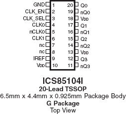
The 85104I is a low skew, high performance 1-to-4 Differential/LVCMOS-to-0.7V HCSL Fanout Buffer. The 85104I has two selectable clock inputs. The CLK0, nCLK0 pair can accept most standard differential input levels. The single-ended CLK1 can accept LVCMOS or LVTTL input levels. The clock enable is internally synchronized to eliminate runt clock pulses on the outputs during asynchronous assertion/deassertion of the clock enable pin. Guaranteed output and part-to-part skew characteristics make the 85104I ideal for those applications demanding well defined performance and repeatability.