
Features
- Two Output Universal Frequency Translator/Frequency Synthesizer
- One programmable as LVPECL or LVDS, One LVCMOS
- Programmable output frequency: 1.0MHz to 250MHz
- Two differential inputs support the following input types: LVPECL, LVDS, LVHSTL, HCSL
- Input frequency range: 8kHz - 710MHz , Crystal input frequency range: 16MHz - 40MHz
- Two factory-set register configurations for power-up default state
- I2C Serial interface for register programming
- RMS phase jitter at 125MHz, using a 40MHz crystal (12kHz - 20MHz): 558fs (typical), Low Bandwidth Mode (FracN)
- RMS phase jitter at 125MHz, using a 100MHz input clock (12kHz - 20MHz): 388fs (typical), High Bandwidth Mode (Integer FB)
- -40\xB0C to 85\xB0C ambient operating temperature
Description
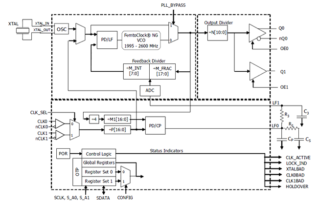
The 849N212I is a highly flexible FemtoClock NG general purpose, low phase noise Universal Frequency Translator / Synthesizer with alarm and monitoring function suitable for networking and communications applications. The 849N212I has three operating modes to support a very broad spectrum of applications: frequency Synthesizer, high-bandwidth frequency translator, and low-bandwidth frequency translator. This device provides two factory-programmed default power-up configurations burned into One-Time Programmable (OTP) memory. To implement other configurations, these power-up default settings can be overwritten after power-up using the I2C interface and the device can be completely reconfigured.
To see other devices in this product family, visit the Universal Frequency Translators page.