
Features
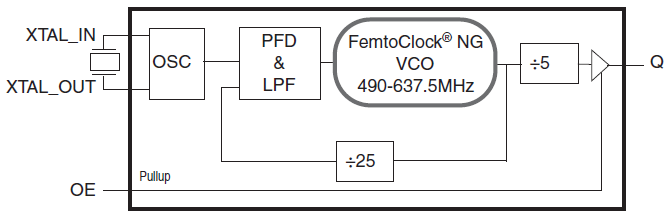
- Fourth generation FemtoClock NG technology
- 125MHz output clock synthesized from a 25MHz fundamental mode crystal
- One 2.5V or 3.3V LVCMOS/LVTTL clock output
- Crystal interface designed for a 12pF parallel resonant crystal
- RMS phase jitter at 125MHz, using a 25MHz crystal (1.875MHz to 20MHz): 0.156ps (maximum)
- RMS phase jitter at 100MHz, using a 20MHz crystal (12kHz to 20MHz): 0.451ps (maximum)
- LVCMOS interface level for the output enable input
- Full 2.5V or 3.3V supply voltage
- Lead-free (RoHS 6) packaging
- -40 °C to 85 °C ambient operating temperature
Description
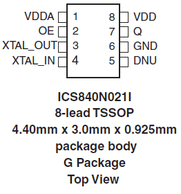
The 840N021 is a LVCMOS/LVTTL clock synthesizer designed for Ethernet applications. The device generates a 125MHz clock signal from a 25MHz crystal with excellent phase jitter performance. The device uses Renesas' fourth generation FemtoClock® NG technology for an optimum of high clock frequency, low phase noise performance and low power consumption. It supports 2.5V or 3.3V voltage supply and is packaged in a small, lead-free (RoHS 6) 8-lead TSSOP package. The extended temperature range supports wireless infrastructure, telecommunication, and networking end equipment requirements.