
Features
- Guaranteed Low Skew < 25ps (max)
- Very low duty cycle distortion < 125ps (max)
- High speed propagation delay < 1.75ns (max)
- Additive phase jitter, RMS 0.159ps (typical) @ 125MHz
- Up to 1GHz operation
- Selectable inputs
- Hot insertable and over-voltage tolerant inputs
- 3.3V / 2.5V LVTTL, HSTL, eHSTL, LVEPECL (2.5V), LVPECL (3.3V), CML, or LVDS input interface
- Selectable differential inputs to six LVDS outputs
- Power-down mode
- 2.5V VDD
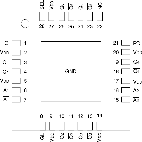
- Available in VFQFPN package
Description
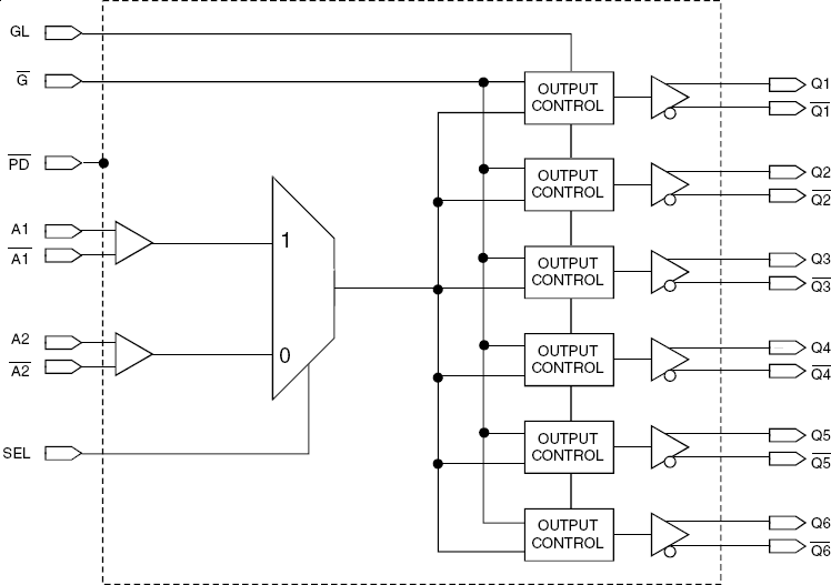
The 5T9306 2.5V differential clock buffer is a user-selectable differential input to six LVDS outputs. The fanout from a differential input to six LVDS outputs reduces loading on the preceding driver and provides an efficient clock distribution network. The 5T9306 can act as a translator from a differential HSTL, eHSTL, LVEPECL (2.5V), LVPECL (3.3V), CML, or LVDS input to LVDS outputs. A single-ended 3.3V / 2.5V LVTTL input can also be used to translate to LVDS outputs. The redundant input capability allows for an asynchronous change-over from a primary clock source to a secondary clock source. Selectable reference inputs are controlled by SEL. The 5T9306 outputs can be asynchronously enabled/disabled. When disabled, the outputs will drive to the value selected by the GL pin. Multiple power and grounds reduce noise.
Parameters
| Attributes | Value |
|---|---|
| Temp. Range (°C) | -40 to 85°C |
| Product Category | Clock Buffers & Drivers, Clock Multiplexers |
Package Options
| Pkg. Type | Pkg. Dimensions (mm) | Lead Count (#) | Pitch (mm) |
|---|---|---|---|
| VFQFPN | 6.0 x 6.0 x 0.85 | 28 | 0.65 |