
Features
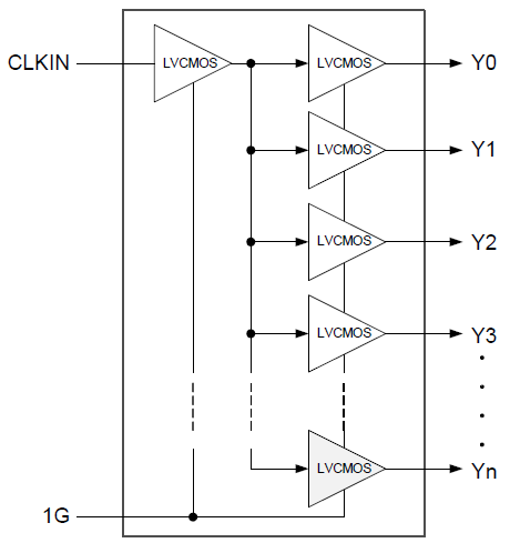
- High-performance 1:10 LVCMOS clock buffer
- Very low pin-to-pin skew: < 50ps
- Very low additive jitter: < 50fs
- Supply voltage: 1.8V to 3.3V
- fMAX = 200MHz
- Integrated serial termination for 50Ω channel
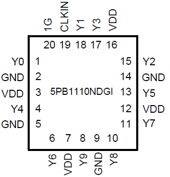
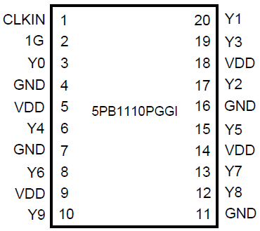
- Packaged in 20-pin TSSOP and small QFN packages
- Extended -40 °C to +105 °C temperature range
- AEC-Q100 qualified, Automotive Grade 2 (-40 °C to +105 °C)


Description
The 5PB1110 is a high-performance 1:10 LVCMOS clock buffer that offers a best-in-class additive phase jitter of 50fs RMS. This clock buffer also supports an Output Enable function. It is available in 20-pin QFN and TSSOP packages and can operate from a 1.8V to 3.3V supply.
Parameters
| Attributes | Value |
|---|---|
| Temp. Range (°C) | -40 to 85°C, -40 to 105°C |
| Product Category | Automotive Timing, Clock Buffers & Drivers |
Applications
- Industrial applications
- Automotive Radar, LiDAR, and other applications