Renesas Electronics Corporation, a premier supplier of advanced semiconductor solutions, unveiled the industry’s first server chipset for next-generation DIMM applications based on Multiplexer Combined Ranks Dual In-line Memory Module (MCR DIMM) technology. Even with the evolution of high-speed DDR5 specifications, many cloud and enterprise applications for in-memory databases, virtual machines and high-performance compute have insatiable appetite for memory bandwidth needs that native DDR5 technology cannot deliver. This is further accentuated due to the break-neck speed at which CPU core count is increasing. To alleviate this acute bottleneck on memory bandwidth, Renesas has collaborated with memory and CPU ecosystem vendors for over three years, playing a key role in architecture and specifications development for the new MCR DIMM sub-system. Further, Renesas designed and executed two critical components – the RG5R188 Multiplexed Registered Clock Driver (MRCD) and the RG5F188 Multiplexed Data Buffer (MDB) – for the new architecture. Both components are available to partners to build the industry’s first memory modules based on MCR DIMM technology.
MCR DIMM technology employs an innovative, and powerful, yet simple concept to achieve significantly higher memory bandwidth. The host side connection to the CPU operates at twice the speed of the standard DDR5 DIMM. DRAM interfaces, however, operate at standard DDR5 speeds but fetch twice the amount of data from the DRAM with point-to-point post-buffer connectivity to the DRAM interface allowing both DRAM ranks servicing data to DB. This allows for the most cost effective and mainstream DRAM to be used for this purpose. Renesas’ MCR DIMM chipset incorporates key functionality that manipulates the data between the host and DRAM interface at +135% bandwidth (BW) improvement over standard RDIMM (at 5600MT/s). It also optimizes signal integrity to achieve higher BW/watt with significant power optimization on the MCR DIMM chipset.
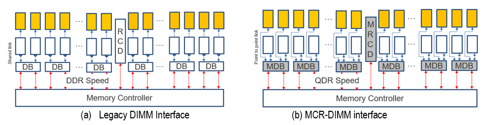
MRCD is a Multiplexed Registered Clock Driver used on MCR DIMMs to buffer the Command/Address (CA) bus, chip selects and clock between the host controller and the DRAMs. It also has a BCOM bus that controls the data buffers. MRCD contains two separate channels with some common logic such as clocking, but which otherwise operate independently of each other. For each channel, the host interface is a 7-bit + parity CA bus with two chip-select inputs. It is double data rate, carries two multiplexed pseudo-channels which can operate in the same direction simultaneously, and runs at twice the frequency of the DRAM interfaces. MRCD demultiplexes the pseudo-channels and transmits each to a separate DRAM output interface. Each DRAM interface is a 14-bit single data rate CA bus output with a chip-select. MRCD also transcodes commands from the CA bus onto a per-channel BCOM bus for data buffer control.
MDB is a Multiplexed Data Buffer to demultiplex and buffer data from the host CPU to DRAMs. It has two 4-bit data interfaces to the host, running at twice the speed of the DRAM interfaces. Each host interface multiplexes two pseudo-channels, both of which have a separate 4-bit DRAM interface. MDB supports x4 or x8 DRAMs. It also has an input-only control bus interface that is connected to an MRCD, as well as a dedicated pin for ZQ calibration and loopback outputs for test purposes.
To learn more about Renesas’ MCR DIMM offerings, visit our DDR5 Solutions page.