
特長
- Optimized for smartphone and notebook/tablet PC applications
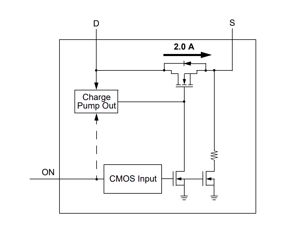
- 15.5mΩ RDSON while supporting 2.0A
- Power supply/input voltage range: 0.85V ≤ VD ≤ 1.9V
- Over-temperature protection
- Output voltage slew-rate internally fixed
- Output discharge circuitry
- Sleep mode current (IDDOFF) in low µA range
SLG59M1551V
説明
The SLG59M1551V single N-channel load switch is designed for load switching applications. The part comes with one 15.5mΩ 2.0A rated MOSFET controlled by a single ON control pin. The product is packaged in an ultra‑small 1.0mm x 1.0mm package.
パラメータ
| 属性 | 値 |
|---|---|
| FET Pass Device Type | Single N-Channel |
| VIN Channel 1 min. (V) | 0.85 |
| VIN Channel 1 max. (V) | 1.9 |
| Input Quiescent Current Channel 1, typ (µA) | 30 |
| Input Quiescent Current Channel 1, max (µA) | 40 |
| Input Quiescent Current when OFF Channel 1, typ (µA) | 0.5 |
| Input Quiescent Current when OFF Channel 1, max (µA) | 1 |
| RDSON (Typ) Channel 1 (mΩ) | 15.5 |
| IDS Channel 1 (A) | 2 |
| Enable | Active High |
| Output Voltage Slew Rate set by | No |
| Discharge Circuit | Yes |
| Undervoltage Protection | No |
| Over Voltage Protection | No |
| Power Good (PG), FAULT indicator | No |
| Reverse current blocking | No |
| Reverse voltage detection | No |
| Over Current Protection (OCP) | No |
| Short Circuit Protection | No |
| Over Temperature Protection (OTP) | Yes |
| Current Monitor Output | No |
| Internal TVS Surge Protection | No |
| Temp. Range (°C) | -40 to +85°C |
Renesas Boards & Kits
SLG59M1551V-EVB
アクティブ
SLG59M1551V Evaluation Board
The SLG59M1551V-EVB board evaluates the SLG59M1551V GreenFET, Single N-Channel, Load Switch.


