特長
- 1パッケージに2つの独立した電源スイッチを搭載
- 電力供給: 2.5 V ≤ VDD ≤ 5.5 V
- 入力電圧範囲: 0.9 V ≤ VD ≤ VDD
- 4.5A/chに対応しながら14.5 mΩ RDSON
- 外付けコンデンサによる出力電圧のスルーレート制御
- 加熱の防止
- 出力放電回路
- フットプリント対応の発注オプション

SLG59M1527V
説明
SLG59M1527Vは、負荷スイッチ用途に設計されています。 この部品は、2つのオンコントロールピンでスイッチングされる2つの4.5A定格のMOSFETを搭載しています。 各MOSFETのオン時間を外付けコンデンサで独立に調整します
パラメータ
| 属性 | 値 |
|---|---|
| FET Pass Device Type | Dual N-Channel |
| VDD min. (V) | 2.5 |
| VDD max. (V) | 5.5 |
| VIN Channel 1 min. (V) | 0.9 |
| VIN Channel 1 max. (V) | 5.5 |
| Input Quiescent Current Channel 1, typ (µA) | 50 |
| Input Quiescent Current Channel 1, max (µA) | 75 |
| Input Quiescent Current when OFF Channel 1, typ (µA) | 0.1 |
| Input Quiescent Current when OFF Channel 1, max (µA) | 1 |
| Input Quiescent Current Channel 2, typ (µA) | 50 |
| Input Quiescent Current Channel 2, max (µA) | 75 |
| Input Quiescent Current when OFF Channel 2, typ (µA) | 0.1 |
| Input Quiescent Current when OFF Channel 2, max (µA) | 1 |
| RDSON (Typ) Channel 1 (mΩ) | 14.5 |
| IDS Channel 1 (A) | 4.5 |
| Enable | Active High |
| Output Voltage Slew Rate set by | Capacitor |
| Discharge Circuit | Yes |
| Undervoltage Protection | No |
| Over Voltage Protection | No |
| Power Good (PG), FAULT indicator | No |
| Reverse current blocking | No |
| Reverse voltage detection | No |
| Over Current Protection (OCP) | Internally Fixed |
| Over Current Protection Setting Range Channel 1 | 6 - 6 |
| Short Circuit Protection | Yes |
| Over Temperature Protection (OTP) | Yes |
| Current Monitor Output | No |
| Internal TVS Surge Protection | No |
| Temp. Range (°C) | -40 to +85°C |
アプリケーション
- S0 +5.0および3.3V電源レールのスイッチON/OFFと、それに伴うサポート回路の放電に最適
- 5V以下の電源レールのON/OFFスイッチに最適
- どちらかのチャネルで最大4.5Aまで、合計最大電流8.5Aまで使用可能
- 各チャネルソース端子の最大負荷容量1000μF
このデバイスに組み合わせたい製品
更に設計開発を進めるための製品を探してみましょう
Renesas Boards & Kits
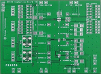
SLG59M1527V-EVB
アクティブ
SLG59M1527V Evaluation Board
The SLG59M1527V-EVB board evaluates the SLG59M1527V GreenFET, Dual N-Channel Load Switch.
For details on how to use the evaluation board, please refer to the evaluation board user manual included in the datasheet.
推奨ドキュメント:
