特長
- 115VDC bootstrap supply maximum voltage supports 100V on the half-bridge
- 3A source and 4A sink gate drivers for NMOS FETs
- Fast propagation delay and matching: 15ns typical delay
- Integrated 0.5Ω typical bootstrap diode
- Wide 6V to 18V operating voltage range
- VDD and boot Undervoltage Lockout (UVLO)
- Robust noise tolerance: wide hysteresis at inputs; HS pin tolerates up to -10V continuous
- Tri-Level PWM input with logic threshold levels set by external VREF pin from 2.7V to 5.5V
- Programmable dead time prevents shoot-through; adjustable from 35ns to 350ns with a single resistor

説明
The HIP2210 is a 100V, 3A source, 4A sink high-frequency half-bridge NMOS FET driver. The HIP2210 features a tri-level PWM input with programmable dead time. Its wide operating supply range of 6V to 18V and integrated high-side bootstrap diode supports driving the high-side and low-side NMOS in 100V half-bridge applications.
This driver features strong 3A source, 4A sink drivers with very fast 15ns typical propagation delay and 2ns typical delay matching, making it optimal for high-frequency switching applications. VDD and boot UVLO protects against an undervoltage operation.
The tri-level input of the HIP2210 PWM pin controls the high-side and low-side drivers with a single pin. When the PWM input is at logic high, the high-side bridge FET is turned on and the low-side FET is off. When the input is at logic low, the low-side bridge FET is turned on and the high-side FET is turned off. When the input voltage is in the mid-level state, both the high-side and low-side bridge FETs are turned off. The PWM threshold levels are proportional to an external input reference voltage on the VREF pin, allowing PWM operation across a 2.7V to 5.5V logic range.
The HIP2210 is offered in a 10 Ld 4x4mm TDFN package.
パラメータ
| 属性 | 値 |
|---|---|
| Bootstrap Supply Voltage (Max) (V) | 115 |
| VBIAS (Max) (V) | 18 |
| Peak Pull-up Current (A) | 3 |
| Peak Pull-down Current (A) | 4 |
| Turn-On Prop Delay (ns) | 15 |
| Turn-Off Prop Delay (ns) | 15 |
| Rise Time (μs) | 0.02 |
| Fall Time | 20 |
| Temp. Range (°C) | -40 to +125°C |
| Input Logic Level | Tri-level |
| Qualification Level | Standard |
| Simulation Model Available | iSim |
パッケージオプション
| Pkg. Type | Pkg. Dimensions (mm) | Lead Count (#) | Pitch (mm) |
|---|---|---|---|
| TDFN | 4.0 x 4.0 x 0.75 | 10 | 0.8 |
アプリケーション
- Telecom half-bridge and full-bridge DC/DC converters
- 3-phase BLDC motor driver; H-Bridge motor driver
- Two-switch forward and active clamp converters
- Multiphase PWM DC/DC controllers
- Class-D amplifiers
Renesas Boards & Kits
100V, 3A Source, 4A Sink, High-Frequency Half-Bridge NMOS FET Drivers
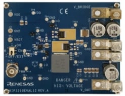
The HIP2210EVAL1Z evaluation board is designed to provide a quick and comprehensive method for evaluating the HIP2210 100V, 3A source, 4A sink, high frequency half-bridge driver for driving the gates of two N-channel MOSFETs in a half-bridge configuration. Two N-channel MOSFETs (with dual... 続きを読む
