特長
- PCIe Gen1-4準拠
- 終端抵抗の内蔵により100Ωの差動Zoを実現:部品点数と基板面積を削減
- 1.8V動作:消費電力の低減
- オプションで1.05V~1.8Vの任意の電圧から出力可能:最大限の省電力を実現
- OE#端子:DIFパワーマネージメント対応
- LP-HCSL差動クロック出力:消費電力と基板面積の削減
- 各出力のスルーレートをプログラマブルに設定可能:様々な線路長に対応したチューニングが可能
- プログラマブル出力振幅:様々なアプリケーション環境に対応したチューニングが可能
- PLLがロックされるまでDIF出力をブロック:クリーンなシステムスタートアップ
- DIF出力のスプレッドは0%、-0.25%、-0.5%から選択可能:EMIの低減
- 外付け25MHz水晶振動子、0ppmの合成誤差でタイトなppmをサポート
- ストラップピンによる構成が可能:デバイス制御のためのSMBusインタフェースは不要
- 3.3VトレラントSMBusインタフェースは、レガシーコントローラに対応
- 6×6 mmの48ピンVFQFPNで、基板面積を最小限に抑えた省スペース設計
- 選択可能なSMBusアドレス:複数のデバイスでSMBusセグメントを簡単に共有
- AEC-Q100準拠、グレード2(-40℃~+105℃)バージョンで提供(ウェッタブルフランクパッケージ)

9FGV0841 - Block Diagram
説明
9FGV0841は、PCIe Gen1–4アプリケーション用の8出力の超低消費電力クロックジェネレータで、Zo=100Ωの出力終端を内蔵しています。 クロック管理用に8つの出力イネーブルを備え、スペクトラム拡散オフに加えて2種類のスペクトラム拡散レベルをサポートします。
評価ボードや材料に関する情報は、お近くの販売代理店にお問い合わせください。
パラメータ
| 属性 | 値 |
|---|---|
| Diff. Outputs | 8 |
| Diff. Output Signaling | LP-HCSL |
| Output Freq Range (MHz) | 25 - 25, 100 - 100 |
| Power Consumption Typ (mW) | 62 |
| Supply Voltage (V) | 1.8 - 1.8 |
| Output Type | LP-HCSL, LVCMOS |
| Xtal Freq (MHz) | 25 - 25 |
| Diff. Termination Resistors | 0 |
| Package Area (mm²) | 36 |
| Battery Backup | No |
| Battery Seal | No |
| CPU Supervisory Function POR | No |
| Crystal Frequency Trimming | No |
| Frequency Out Pin | No |
| Inputs (#) | 1 |
| Input Freq (MHz) | 25 - 25 |
| Function | Generator |
| Input Type | Crystal, LVCMOS |
| Core Voltage (V) | 1.8 |
| Output Voltage (V) | 0.8V, 1.8V |
| Product Category | Automotive Timing, PCI Express Clocks |
パッケージオプション
| Pkg. Type | Pkg. Dimensions (mm) | Lead Count (#) | Pitch (mm) |
|---|---|---|---|
| VFQFPN | 6.0 x 6.0 x 0.9 | 48 | 0.4 |
アプリケーション・ブロック図
 | コネクテッドAndroidベースの車両インストルメントクラスタ ワイヤレス接続とリアルタイムディスプレイを備えたAndroidベースの自動車コックピット。 |
 | 通信ゲートウェイおよび統合DVR/DMSシステム CoGWとDVR/DMSビデオ処理を統合した統合車載ゲートウェイ。 |
 | ハプティクスを備えた自動車コックピットシステム 次世代の触覚、BroadLEDドライバ、PMICを備えた高度なコックピットシステム。 |
 | タイヤ空気圧監視システム PMICを内蔵した低電力Bluetooth LE TPMS設計により、コスト、サイズ、開発時間を短縮します。 |
 | フルグラフィックス クラスタ&コックピットシステム 自動車のコックピットでフルグラフィックス クラスタをサポートする高効率ディスプレイシステム。 |
 | ハイエンドコックピット&インフォテインメントソリューション |
 | 4Kビデオをサポートするフル機能HMI 高性能HMI設計により、シームレスな4Kビデオ、高度なグラフィックス、および信頼性の高いコネクティビティを実現します。 |
 | FHDビデオをサポートするフル機能HMI フル機能のHMIプラットフォームは、高性能MPUを備え、USB 3.0、PCI Express、およびギガビットイーサネットインタフェースを内蔵しています。 |
このデバイスに組み合わせたい製品
更に設計開発を進めるための製品を探してみましょう
Renesas Boards & Kits
RTP8A779G0ASKB0FS0SA000
アクティブ
R-Car V4Hシステム評価ボードセット/White Hawk
White Hawkは、R-Car V4H搭載システムの評価や、OS、デバイスドライバ、アプリケーション開発に使用できるR-Car V4H専用評価ボードセットです。 White Hawkボードセットを使用することで、R-Car V4Hのシステム性能評価などに必要な作業を効率的に実施でき、製品開発期間を大幅に短縮できます。
本ボードは、高解像度4Kを含むマルチカメラ入力、4Kディスプレイ出力、オーディオ出力、ネットワーク通信インタフェース、および複数の電子制御ユニット(ECU)の並列動作に対応するPCIe Gen4をサポートしています。
RTP0RC77990SEB0010S
アクティブ
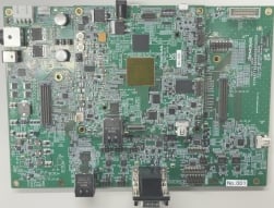
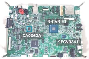
フルグラフィックスクラスタ&コックピットソリューション R-Car E3開発ボード/Ebisu
R‑Car E3とクロックジェネレータの組み合わせにより、エントリー車向け統合型コックピットの大型パネルに対応したフルグラフィックスクラスタソリューションに最適な機能と性能を提供します。 本開発ボードを使用することで、開発者はR‑Car E3システムオンチップ(SoC)の評価を行い、ハードウェアおよびソフトウェアソリューションの開発を迅速に開始できます。

RTP0RC7795SIPB0012S
アクティブ
ハイエンドコックピット&インフォテインメントソリューション R‑Car H3/M3開発ボード/Salvator‑XS
R‑Car(H3/M3/M3N)SiP(System in Package)とクロックジェネレータの組み合わせにより、幅広いディスプレイ出力と高品質な性能を維持しつつ、高効率を実現し、拡張性のあるコックピットおよびインフォテインメントソリューションに最適です。
このボードをリモートでテストする
クラウド上のラボで利用でき、PCベースのGUIを使用して、物理ボードを必要とせずに、仮想ラボで設計の構成とテストをすぐに開始できます。
Partner Boards & Kits
SoM/SBC
RZ/G2 Series System on Module (SoM)
Beacon EmbeddedWorks' RZ/G2 series of system on modules (SoMs) deliver high-performance and full-featured capabilities for demanding embedded applications. Configurable from dual-core to octa-core, they include on-board Wi-Fi® 5, Bluetooth® 4.2, and LTE Cat M1/NB1. This flexibility in performance and connectivity simplifies developing a portfolio of secure devices on a single hardware design—perfectly suited for high-performance multimedia processing including 3D graphics, HD video, and displays for medical, military, aerospace, and industrial applications.
Provided By:
Beacon EmbeddedWorks


