
| CADモデル: | View CAD Model |
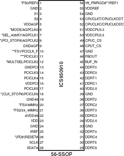
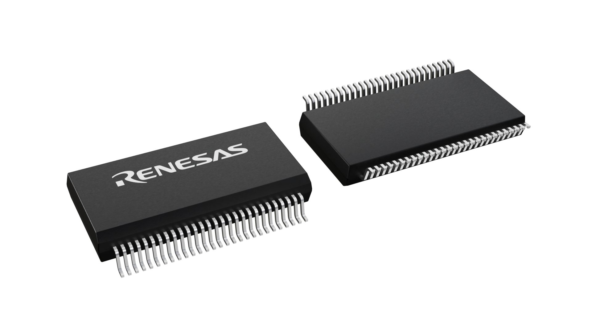
| Pkg. Type: | SSOP |
| Pkg. Code: | PVG56 |
| Lead Count (#): | 56 |
| Pkg. Dimensions (mm): | 18.4 x 7.5 x 2.3 |
| Pitch (mm): | 0.64 |
| Pb (Lead) Free | Yes |
| Moisture Sensitivity Level (MSL) | 1 |
| ECCN (US) | |
| HTS (US) |
| Pkg. Type | SSOP |
| Lead Count (#) | 56 |
| Pb (Lead) Free | Yes |
| Carrier Type | Reel |
| C-C Jitter Max P-P (ps) | 100 |
| Chipset Manufacturer | VIA |
| Core Voltage (V) | 2.5V, 3.3V |
| Feedback Input | No |
| Function | Clock Generator |
| Input Freq (MHz) | 14.318 - 14.318 |
| Input Type | Crystal |
| Inputs (#) | 2 |
| Length (mm) | 18.4 |
| MOQ | 1000 |
| Moisture Sensitivity Level (MSL) | 1 |
| Output Banks (#) | 8 |
| Output Freq Range (MHz) | 14.32 - 14.32, 33.33 - 33.33, 66.66 - 66.66, 48 - 200 |
| Output Skew (ps) | 100 |
| Output Voltage (V) | 2.5V, 3.3V |
| Package Area (mm²) | 138 |
| Pb Free Category | e3 Sn |
| Period Jitter Max P-P (ps) | 250 |
| Pitch (mm) | 0.64 |
| Pkg. Dimensions (mm) | 18.4 x 7.5 x 2.3 |
| Prog. Clock | Yes |
| Prog. Interface | I2C |
| Qty. per Carrier (#) | 0 |
| Qty. per Reel (#) | 1000 |
| Reel Size (in) | 13 |
| Reference Output | Yes |
| Requires Terms and Conditions | Does not require acceptance of Terms and Conditions |
| Spread Spectrum | Yes |
| Tape & Reel | Yes |
| Temp. Range (°C) | 0 to 70°C |
| Thickness (mm) | 2.3 |
| Width (mm) | 7.5 |
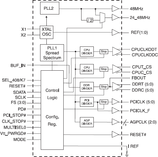
The 950910 is a single chip clock solution for desktop designs using the VIA P4X/P4M/KT/KN266/333 style chipsets with PC133 or DDR memory. The 950910 is part of a whole new line of ICS clock generators and buffers called TCH™ (Timing Control Hub). This part incorporates ICS's newest clock technology which offers more robust features and functionality. Employing the use of a serially programmable I2C interface, this device can adjust the output clocks by configuring the frequency setting, the output divider ratios, selecting the ideal spread percentage, the output skew, the output strength, and enabling/disabling each individual output clock. M/N control can configure output frequency with resolution up to 0.1MHz increment.
