特長
- Dual differential outputs
- Output frequency range: 34.375MHz to 4400MHz (continuous range)
- RF output divided by 1, 2, 4, 8, 16, 32, 64
- Open drain outputs (see output distribution section in the datasheet)
- Fractional-N feedback divider (also supports Integer-N mode)
- 16-bit integer and 12-bit fractional (16-bit fractional when using the extended registers)
- 3- or 4-wire SPI interface (compatible with 3.3V and 1.8V)
- Single 3.3V supply
- Logic compatibility: 1.8V
- Integrated high-performance low dropout regulators (LDOs) for excellent power supply noise rejection
- Programmable output power level: -4dBm to +5dBm (up to +7 when using the extended registers)
- Mute function
- Ultra-low phase noise (typical phase noise for 1.65GHz LO: -142.21dBc/Hz at 1MHz offset)
- Lock detect indicators
- Input reference frequency: 5MHz to 310MHz
- 32-lead, 5mm x 5mm VFQFN package
- Automatic VCO band selection (autocal feature)
- -40 °C to +85 °C ambient operating temperature
- Supports +105 °C case temperature
- Lead-free (RoHS 6) packaging


説明
The 8V97053L is a high-performance GSM1800 grade wideband RF synthesizer/PLL optimized for use as the local oscillator (LO) in multi-carrier, multi-mode FDD and TDD base station radio cards. It is offered in a compact 5mm x 5mm, 32-VFQFN package.
The 8V97053L wideband RF synthesizer/PLL offers a default Fractional mode with the option for an Integer mode. It requires an external loop filter.
The 8V97053L has an integrated voltage-controlled oscillator (VCO), supports output frequencies from 34.375MHz to 4400MHz, and maintains superior phase noise and spurious performance.
RF_OUT[A:B] output drivers have independently programmable output power ranging from –4dBm to +7dBm. The RF_OUT outputs can be muted. The mute function is accessible via an SPI command or mute pin.
Renesas Boards & Kits
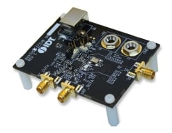
High-Performance Wideband Fractional RF Synthesizer/PLL Evaluation Kit
The 8V97053L-EVK evaluation kit is designed to help the customer evaluate the 8V97053L RF synthesizer/phase-locked loop (PLL). When the board is connected to a PC running Timing Commander™ through USB, the device can be configured and programmed through a Graphical User Interface (GUI) or... 続きを読む
Available Modular Designs by X-Microwave:
XM-A7F4-0609D Phase Lock Loops with Int VCO
サポートコミュニティ
-
ルネサスのクロックチップのスイング範囲と最小調整ステップの見方について
... 動的に調整できます。 4つの製品を見つけましょう:8V97003,8V97051L,8V97052,8V97053L。 クロックのスイング範囲や最小ステップはどうやって ...
2024年8月14日


