
特長
- Three LVPECL output pairs
- Frequency divide select options: ÷2, ÷4, ÷8, ÷16 (Bank B)
- Pass-through output (Bank A)
- IN, nIN input can accept the following differential input levels: LVPECL, LVDS, CML
- Output frequency: 2.5GHz
- Bank skew: 40ps (maximum), Bank B
- Part-to-part skew: 230ps (maximum)
- Additive phase jitter, RMS: 0.15ps (typical)
- Voltage supply range: 2.375V to 3.6V
- -40°C to 85°C ambient operating temperature
- Available in lead-free (RoHS 6) package
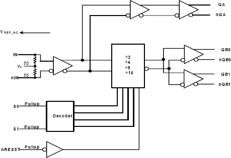
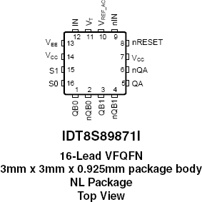
8S89871I - Block Diagram
説明
The 8S89871 is a high speed Differential-to-LVPECL Buffer/Divider. The 8S89871 has a selectable ÷2, ÷4, ÷8, ÷16 output dividers. The clock input has internal termination resistors, allowing it to interface with several differential signal types while minimizing the number of required external components. The device is packaged in a small, 3mm x 3mm VFQFN package, making it ideal for use on space-constrained boards.


