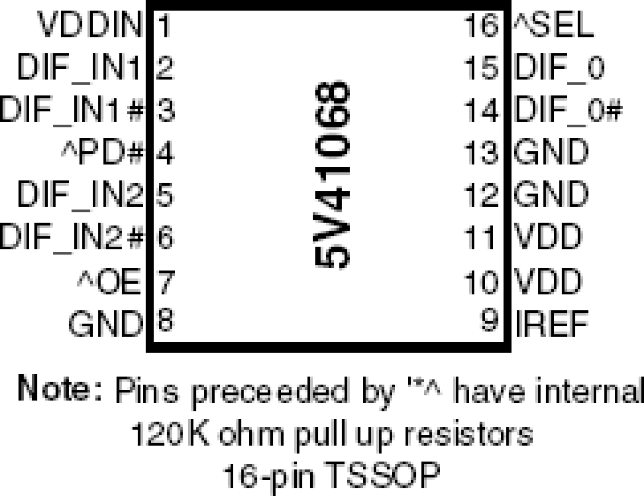
パッケージ情報
| CADモデル: | View CAD Model |
| Pkg. Type: | TSSOP |
| Pkg. Code: | PGG16 |
| Lead Count (#): | 16 |
| Pkg. Dimensions (mm): | 5.0 x 4.4 x 1.0 |
| Pitch (mm): | 0.65 |
環境及び輸出分類情報
| Moisture Sensitivity Level (MSL) | 1 |
| Pb (Lead) Free | Yes |
| ECCN (US) | EAR99 |
| HTS (US) | 8542.39.0090 |
製品スペック
| Lead Count (#) | 16 |
| Carrier Type | Tube |
| Moisture Sensitivity Level (MSL) | 1 |
| Qty. per Reel (#) | 0 |
| Qty. per Carrier (#) | 96 |
| Pb (Lead) Free | Yes |
| Pb Free Category | e3 Sn |
| Temp. Range (°C) | 0 to 70°C |
| Accepts Spread Spec Input | Yes |
| Additive Phase Jitter Typ RMS (fs) | 100 |
| Additive Phase Jitter Typ RMS (ps) | 0.1 |
| App Jitter Compliance | PCIe Gen1, PCIe Gen2, PCIe Gen3 |
| Architecture | Common |
| Core Voltage (V) | 3.3 |
| Diff. Input Signaling | HCSL |
| Diff. Inputs | 2 |
| Diff. Output Signaling | HCSL |
| Diff. Outputs | 1 |
| Diff. Termination Resistors | 4 |
| Function | Multiplexer |
| Input Freq (MHz) | 200 |
| Input Type | HCSL |
| Inputs (#) | 2 |
| Length (mm) | 5 |
| MOQ | 192 |
| Output Banks (#) | 1 |
| Output Freq Range (MHz) | 200 |
| Output Type | HCSL, LVDS |
| Output Voltage (V) | 3.3 |
| Outputs (#) | 1 |
| PLL | No |
| Package Area (mm²) | 22 |
| Pitch (mm) | 0.65 |
| Pkg. Dimensions (mm) | 5.0 x 4.4 x 1.0 |
| Pkg. Type | TSSOP |
| Power Consumption Typ (mW) | 132 |
| Price (USD) | $10.10168 |
| Product Category | Clock Multiplexers, PCI Express Clocks |
| Prog. Clock | No |
| Requires Terms and Conditions | Does not require acceptance of Terms and Conditions |
| Supply Voltage (V) | 3.3 - 3.3 |
| Tape & Reel | No |
| Thickness (mm) | 1 |
| Width (mm) | 4.4 |
5V41068A に関するリソース
説明
The 5V41068A is a 2:1 differential clock mux for PCI Express applications. It has very low additive jitter making it suitable for use in PCIe Gen2 and Gen3 systems. The 5V41068A selects between 1 of 2 differential HCSL inputs to drive a single differential HCSL output pair. The output can also be terminated to LVDS.


