
| CADモデル: | View CAD Model |
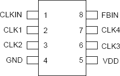
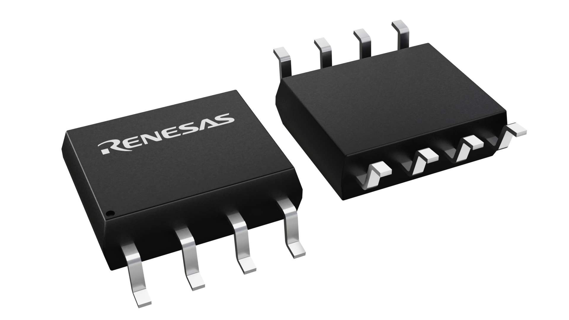
| Pkg. Type: | SOIC |
| Pkg. Code: | DCG8 |
| Lead Count (#): | 8 |
| Pkg. Dimensions (mm): | 4.9 x 3.9 x 1.5 |
| Pitch (mm): | 1.27 |
| Moisture Sensitivity Level (MSL) | 1 |
| Pb (Lead) Free | Yes |
| ECCN (US) | EAR99 |
| HTS (US) | 8542.39.0090 |
| Lead Count (#) | 8 |
| Carrier Type | Reel |
| Moisture Sensitivity Level (MSL) | 1 |
| Qty. per Reel (#) | 3000 |
| Qty. per Carrier (#) | 0 |
| Pb (Lead) Free | Yes |
| Pb Free Category | e3 Sn |
| Temp. Range (°C) | 0 to 70°C |
| Advanced Features | Feedback Input, Spread Spectrum |
| C-C Jitter Max P-P (ps) | 250 |
| Core Voltage (V) | 3.3V, 5V |
| Feedback Input | Yes |
| Input Freq (MHz) | 20 - 160 |
| Input Type | LVCMOS |
| Inputs (#) | 1 |
| Length (mm) | 4.9 |
| MOQ | 3000 |
| Output Banks (#) | 1 |
| Output Freq Range (MHz) | 20 - 160 |
| Output Skew (ps) | 150 |
| Output Type | LVCMOS |
| Output Voltage (V) | 3.3V, 5V |
| Outputs (#) | 4 |
| Package Area (mm²) | 19.1 |
| Period Jitter Typ P-P (ps) | 170 |
| Pitch (mm) | 1.27 |
| Pkg. Dimensions (mm) | 4.9 x 3.9 x 1.5 |
| Pkg. Type | SOIC |
| Price (USD) | $10.4597 |
| Product Category | Zero Delay Buffers |
| Prog. Clock | No |
| Reel Size (in) | 13 |
| Reference Output | No |
| Requires Terms and Conditions | Does not require acceptance of Terms and Conditions |
| Spread Spectrum | Yes |
| Tape & Reel | Yes |
| Thickness (mm) | 1.5 |
| Width (mm) | 3.9 |
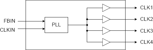
The 574 is a low jitter, low-skew, high performance PLL-based zero delay buffer for high speed applications. Based on IDT's proprietary low jitter Phase Locked Loop (PLL) techniques, the device provides four low skew outputs at speeds up to 160 MHz at 3.3 V. When one of the outputs is connected directly to FBIN, the rising edge of each output is aligned with the rising edge of the input clock. External delay elements connected in the feedback loops will cause the outputs to occur before the inputs by the amount of propagation delay of the external element.
