特長
- Low additive phase jitter RMS: 50fs
- Extremely low skew outputs (50ps)
- Low-cost clock buffer
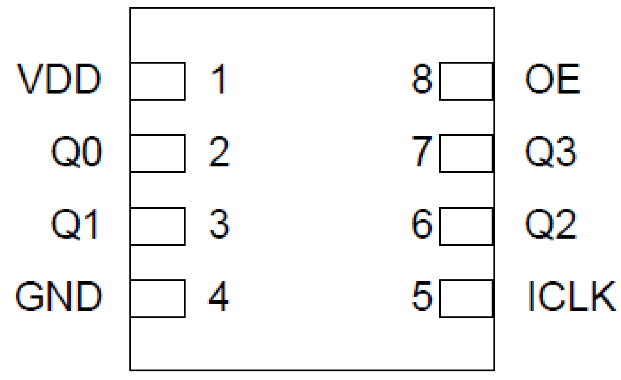
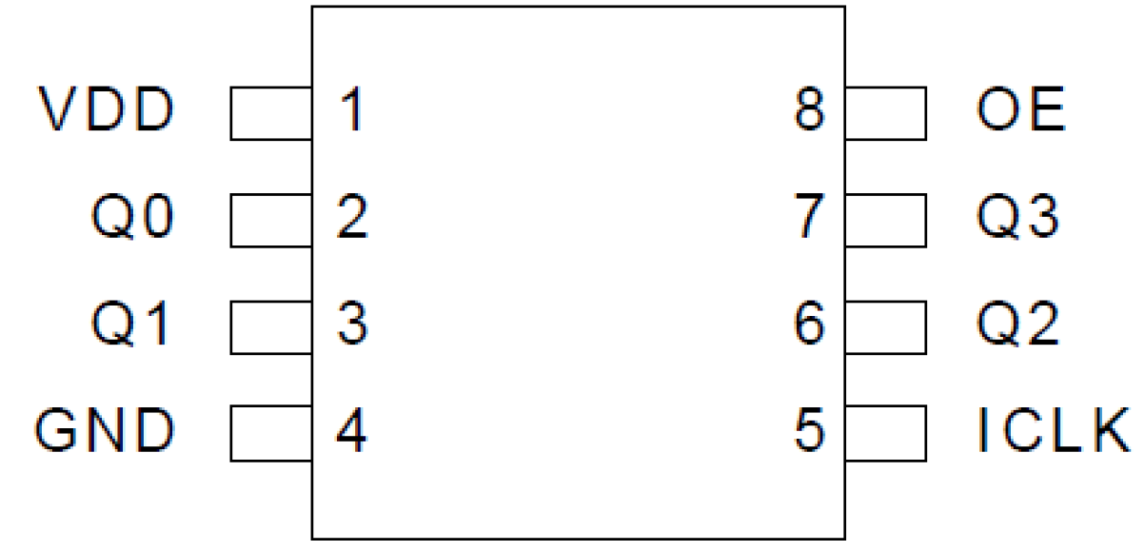
- Packaged in 8-pin SOIC and small 8-pin DFN packages, Pb-free
- Input/Output clock frequency up to 200MHz
- Ideal for networking clocks
- Operating voltages: 1.8V to 3.3V
- Output Enable mode tri-state outputs
- Advanced, low-power CMOS process
- Extended temperature range: -40 °C to +105 °C
説明
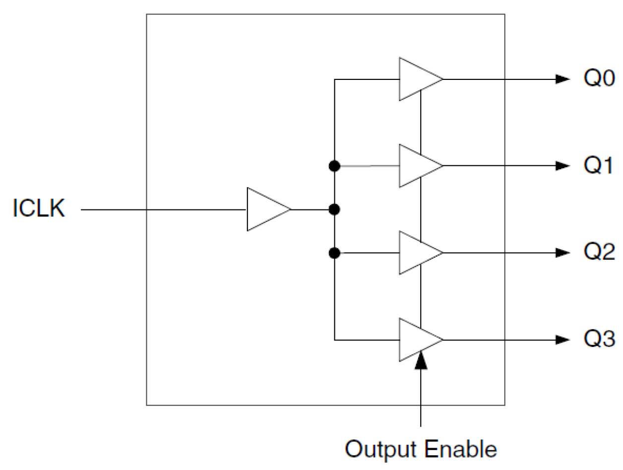
The 553S is a low skew, single input to four output, LVCMOS clock buffer that offers a best-in-class additive phase jitter of sub 50fs.
パラメータ
| 属性 | 値 |
|---|---|
| Temp. Range (°C) | -40 to 85°C |
| Product Category | Clock Buffers & Drivers |
適用されたフィルター


