
| CAD Model: | View CAD Model |
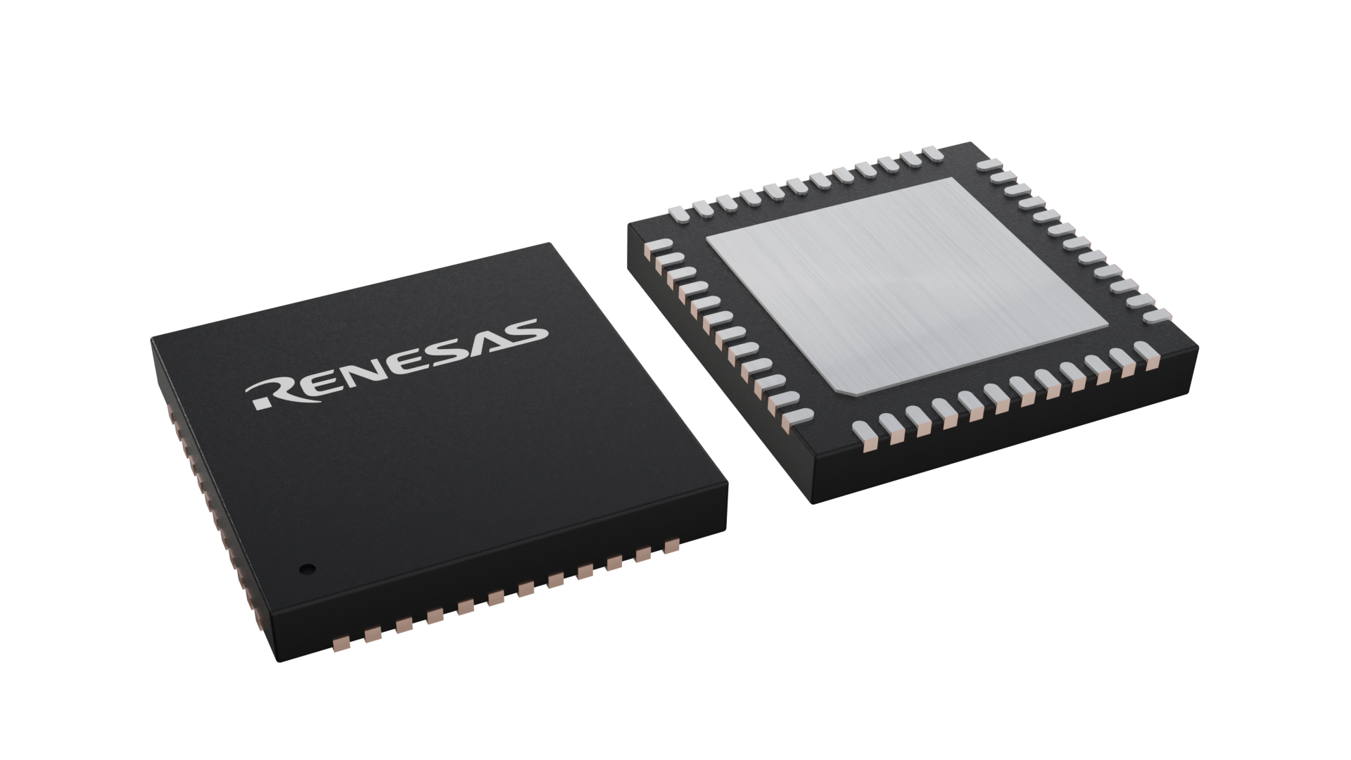
| Pkg. Type: | VFQFPN |
| Pkg. Code: | QV0048AC |
| Lead Count (#): | 48 |
| Pkg. Dimensions (mm): | 6.0 x 6.0 x 0.9 |
| Pitch (mm): | 0.4 |
| Moisture Sensitivity Level (MSL) | 3 |
| Pb (Lead) Free | Yes |
| ECCN (US) | |
| HTS (US) |
| Pkg. Type | VFQFPN |
| Lead Count (#) | 48 |
| Carrier Type | Tray |
| Moisture Sensitivity Level (MSL) | 3 |
| Pkg. Dimensions (mm) | 6.0 x 6.0 x 0.9 |
| Qty. per Reel (#) | 0 |
| Diff. Outputs | 12 |
| Input Type | LVCMOS, CML, LVDS, HCSL, LVPECL, Crystal |
| Outputs (#) | 24 |
| Package Area (mm²) | 36 |
| Qty. per Carrier (#) | 490 |
| Pb (Lead) Free | Yes |
| Pb Free Category | e3 Sn |
| Temp. Range (°C) | -40 to 105°C |
| Advanced Features | Spread Spectrum, Hitless Switching |
| App Jitter Compliance | PCIe Gen1, PCIe Gen2, PCIe Gen3, PCIe Gen4, PCIe Gen5, PCIe Gen6, PCIe Gen7 |
| Application | Switches, Routers, Synchronous Ethernet, Telecom, Jitter Attenuator for PHY or Switches |
| Architecture | Common, SRIS, SRNS |
| Core Voltage (V) | 1.8V, 2.5V, 3.3V |
| Diff. Inputs | 2 |
| Diff. Output Signaling | LP-HCSL, LVDS, LVPECL, LVCMOS |
| Family Name | VersaClock® 8 |
| Fractional Output Dividers (#) | 3 |
| Function | Synthesizer/Jitter Attenuator |
| Input Freq (MHz) | 650, 150 |
| Inputs (#) | 2 |
| Length (mm) | 6 |
| MOQ | 490 |
| Output Banks (#) | 7 |
| Output Freq Range (MHz) | 0.008 - 650 |
| Output Impedance | 34, 85, 100 |
| Output Type | LVDS, LP-HCSL, LVCMOS, LVPECL |
| Output Voltage (V) | 1.8V, 2.5V, 3.3V |
| Phase Jitter Typ RMS (fs) | 102 |
| Pitch (mm) | 0.4 |
| Price (USD) | $7.94641 |
| Product Category | VersaClock, Jitter Attenuators, Network Synchronization, PCI Express Clocks, Programmable Clocks |
| Prog. Clock | Yes |
| Prog. Interface | OTP, I2C, SPI, SMBUS, EEPROM |
| Reference Output | No |
| Requires Terms and Conditions | Does not require acceptance of Terms and Conditions |
| Spread Spectrum | Yes |
| Supply Voltage (V) | 1.8 - 1.8, 2.5 - 2.5, 3.3 - 3.3 |
| Tape & Reel | No |
| Thickness (mm) | 0.9 |
| Width (mm) | 6 |
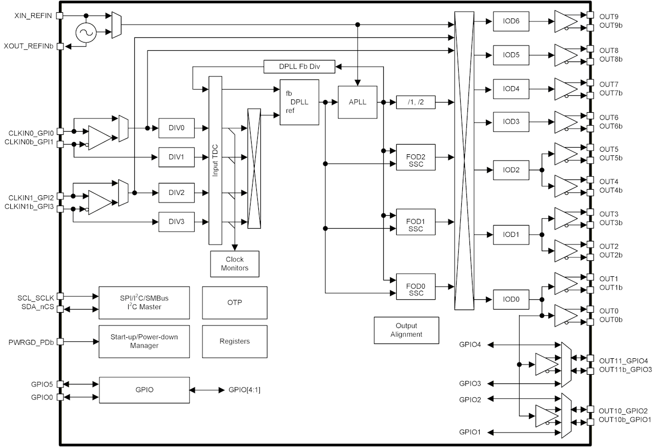
The RC313xxA (RC31312A and RC31309A) is a member of Renesas' VersaClock® 8 programmable clock generator/jitter attenuator family. The device is comprised of a programmable fractional-N DPLL for ultra-low phase noise clocking and jitter attenuation, and an Analog PLL (APLL) driving three independent programmable fractional output dividers (FOD) and individual IODs on each of the seven output banks. The devices can simultaneously provide low-phase jitter non-spreading clocks for Ethernet and storage applications and spread-spectrum PCIe Gen7 clocks.
Up to 18 configurations reusable across multiple designs may be stored in on-chip One-Time Programmable (OTP) memory or external I2C EEPROM. Redundant input is available for backup and used as a reference clock where needed.
