Features
- Single 1.7V - 2.0V Supply
- 128Mbit (16 x 8 Mbit physical block) Flash Memory
- Serial Peripheral Interface (SPI) and Quad Peripheral Interface (QPI) Compatible
- Supports SPI Modes 0 and 3
- Supports Dual Output Read and Quad I/O Program and Read
- Supports QPI Program and Read
- 133MHz Maximum Operating Frequency
- Clock-to-Output (tV1 ) of 6ns
- Up to 65Mbytes/s Continuous Data Transfer Rate
- Quad Enabled
- Full Chip Erase
- Flexible, Optimized Erase Architecture for Code and Data Storage Applications
- 0.6ms Typical Page Program (256 bytes) Time
- 60ms Typical 4kB Block Erase Time
- 200ms Typical 32kB Block Erase Time
- 350ms Typical 64kB Block Erase Time
- Hardware Controlled Locking of Status Registers via WP Pin
- 4kbit Secured One-Time Programmable Security Register
- Hardware Write Protection
- Serial Flash Discoverable Parameters (SFDP) Register
- Flexible Programming
- Byte/Page Program (1 to 256 bytes)
- Dual or Quad Input Byte/Page Program (1 to 256 bytes)
- Erase/Program Suspend and Resume
- JEDEC Standard Manufacturer and Device ID Read Methodology
- Low Power Dissipation
- 2μA Deep Power-Down Current (Typical)
- 10μA Standby Current (Typical)
- 5mA Active Read Current (Typical)
- Endurance: 100,000 program/erase cycles (4kbyte, 32kbyte, or 64kbyte blocks)
- Data Retention: 20 Years
- Industrial Temperature Range: -40°C to +85°C
- Industry Standard Green (Pb/Halide-free/RoHS-Compliant) Package Options
- 8-Pad DFN (6mm x 5mm x 0.6mm)
- 8-Lead SOIC (208mil)
- 21-Ball WLCSP
- 21-Ball Low-Profile WLCSP

Description
The AT25QL128A is a member of our standard class code and data storage solutions designed for low-voltage systems in which program code is shadowed from Flash memory into embedded or external RAM for execution.
The architecture includes standard erase block sizes and a security register for unique device serialization, system-level Electronic Serial Number (ESN) storage, locked key storage, etc.
The AT25QL128A is Quad enabled at the factory and offers a universally compatible pinout and command set, standard block architecture, and continuous read, wrap, and burst modes for XiP.
Renesas Boards & Kits

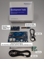
Evaluation Board Kit for RZ/G2UL MPU
This evaluation board kit is ideal for evaluating RZ/G2UL. The RZ/G2UL Evaluation Board Kit consists of a module board (SOM) and a carrier board. The module board complies with the SMARC v2.1 standard.
Contents:
- RZ/G2UL Module Board (SMARC2.1)
- Common Carrier Board (For RZ/G2L, RZ/G2LC, RZ/G2UL and... Read More
RZ/A3UL Evaluation Board Kit
This evaluation board kit is ideal for evaluating RZ/A3UL. The RZ/A3UL Evaluation Board Kit consists of a module board (SOM) and a carrier board. The module board complies with the SMARC v2.1 standard.
Two types of evaluation boards are available: QSPI version and Octal-SPI version.
- QSPI version:... Read More
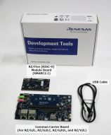
Evaluation Board Kit for RZ/Five MPU
The RZ/Five evaluation kit (EVK) is ideal for evaluating and developing with the Renesas RZ/Five MPU. The EVK includes the RZ/Five SMARC v2.1 System on Module (SoM) and its carrier board. The module board complies with the SMARC v2.1 standard.
- Contents
- RZ/Five (RISC-V) Module Board...
Filters
Partner Solutions
 Development ToolµISP is a compact standalone and universal solution, specifically designed for production environments, based on Algocrafts WriteNow! Technology. This is a standard tool for many families and devices and supports multi programming protocol (JTAG, SPI, UART, DAP, SWD, I2C, BDM, custom protocol, etc).Provided By: Algocraft Srl
- Development ToolWriteNow! Series of In-System Programmers is a breakthrough in the programming industry. The programmers support a large number of devices (microcontrollers, memories, CPLDs and other programmable devices) from various manufacturers and have a compact size for easy ATE/fixture integration. They work in standalone or connected to a ...Provided By: Algocraft Srl
No Results Found.
Make sure all keywords are spelled correctly.
Try fewer, different, or more general terms to vary your search.
If you have filters applied, consider deselecting some to broaden your results.
- Search our extensive knowledgebase, designed to help customers with their FAQs.
- Get help from our expert Renesas technical staff and community on our support forums.
- Development ToolµISP is a compact standalone and universal solution, specifically designed for production environments, based on Algocrafts WriteNow! Technology. This is a standard tool for many families and devices and supports multi programming protocol (JTAG, SPI, UART, DAP, SWD, I2C, BDM, custom protocol, etc).Provided By: Algocraft Srl
- Development ToolWriteNow! Series of In-System Programmers is a breakthrough in the programming industry. The programmers support a large number of devices (microcontrollers, memories, CPLDs and other programmable devices) from various manufacturers and have a compact size for easy ATE/fixture integration. They work in standalone or connected to a ...Provided By: Algocraft Srl
Partner Solutions (2)
Support Communities
-
Request for Linux Kernel Modules for DA16600MOD UART Interface (Wi-Fi and BLE) Integration with RZG3S
Hello Renesas Community, We are currently working on integrating the DA16600MOD Wi-Fi and Bluetooth module into our custom-made system that uses the RZG3S processor. Our system is designed to use only the UART interface to interface with the DA16600MOD for Wi-Fi (UART0) and BLE communication. Could anyone ...
Jan 9, 2025

Support Communities


