Renesas Electronics Corporation - June is Pride Month, a month to raise awareness of the rights and the culture of the LGBTQ+ community

Features

  • 400 - 500 MHz clock source
  • 4 open-drain differential output drives with short term jitter < 40ps
  • Spread spectrum compatible
  • Reference clock is differential or single-ended, 100 or 133 MHz
  • SMBus programmability for: - frequency multiplier - output enable - operating mode
  • Supports frequency multipliers of: 3, 4, 5, 6, 8, 9/2, 15/2 and 15/4
  • Support systems where XDR subsystem is asynchronous to other system clocks
  • 2.5V power supply

Description

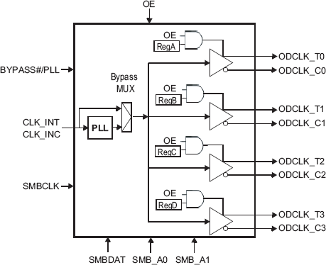
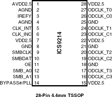
The 9214 clock generator provides the necessary clock signals to support the Rambus XDRTM memory subsystem and Redwood logic interface. The clock source is a reference clock that may or may not be modulated for spread spectrum. The 9214 provides 4 differential clock pairs in a space saving 28-pin TSSOP package and provides an off-the-shelf high-performance interface solution. Figure 1 shows the major components of the 9214 XDR Clock Generator. These include the a PLL, a Bypass Multiplexer and four differential output buffers. The outputs can be disabled by a logic low on the OE pin. An output is enabled by the combination of the OE pin being high, and 1 in its SMBus Output control register bit. The PLL receives a reference clock, CLK_INT/C and outputs a clock signal at a frequency equal to the input frequency times a multiplier. Table 2 shows the multipliers selectable via the SMBus interface. This clock signal is then fed to the differential output buffers to drive the enabled clocks. Disabled outputs are set to Hi-Z. The Bypass mode routes the input clock, CLK_INT/C, directly to the differential output buffers, bypassing the PLL. Up to four 9214 devices can be cascaded on the same SMBus. Table 3 shows the SMBus addressing and control for the four devices.

Part NumberStatusSamplesStockPackageLead Count (#)Temp. GradePb (Lead) FreeCarrier Type
9214DGLFObsoleteN/AOut of StockTSSOP28#CYesTube
9214DGLFTObsoleteN/AOut of StockTSSOP28#CYesReel

Support Communities

  1. DA14531 USB Dialog EVK kit with UART2

    Hi, I have tried samples of Timer0_General and Blinky works fine over changing GPIO Tx pin (05) and UART (SW debug) interface. I want to same application over UART2, how can I configure the Mikcrobus socket and how to connect Rx point of UART receiver on which socket hole ...

    Dec 16, 2021
  2. DA14531 USB Dialog EVK kit does not gives UART2 log.

    Hi, I'm using the TIMER0_general example of (SDK 6.0.2) on DA14531-00FXDEVKT-U, I tried DIP UART2 wire and 4wire enabling condition, And connected TTL to USB from EVK to my PC to read the UART print but I could not see any printf_string logs ...

    Dec 15, 2021
  3. How to change bluetooth name correctly?

    char         USER_DEVICE_NAME[]    =    "BLUE-XXXXXX"; uint8_t      USER_DEVICE_NAME_LEN  =    (sizeof(USER_DEVICE_NAME)-1); void user_app_init(void) {         sprintf(USER_DEVICE_NAME+4,"%2X%2X%2X",dev_bdaddr.addr[2],dev_bdaddr.addr[1],dev_bdaddr.addr[0]);      app_param_update_request_timer_used = EASY_TIMER ...

    Dec 16, 2021
View All Results from Support Communities (6)
Support Communities

Support Communities

Get quick technical support online from Renesas Engineering Community technical staff.
Browse Articles

Knowledge Base

Browse our knowledge base for helpful articles, FAQs, and other useful resources.
Submit a Ticket

Submit a Ticket

Need to ask a technical question or share confidential information?