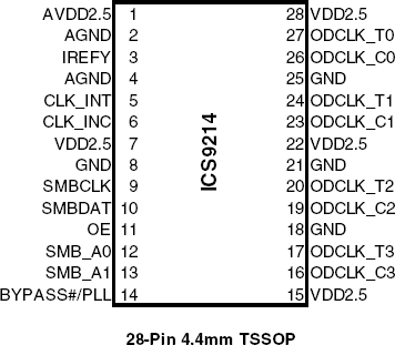
| Lead Count (#) | 28 |
| Pkg. Type | TSSOP |
| Pkg. Code | PGG28 |
| Pitch (mm) | 0.65 |
| Pkg. Dimensions (mm) | 9.7 x 4.4 x 1.0 |
| Pb (Lead) Free | Yes |
| ECCN (US) | EAR99 |
| HTS (US) | 8542.39.0090 |
| Moisture Sensitivity Level (MSL) | 1 |
| Pkg. Type | TSSOP |
| Lead Count (#) | 28 |
| Pb (Lead) Free | Yes |
| Carrier Type | Tube |
| C-C Jitter Max P-P (ps) | 250 |
| Chipset Manufacturer | RAMBUS |
| Clock Spec. | XDR |
| Core Voltage (V) | 3.3 |
| Function | Buffer |
| Input Freq (MHz) | 14.32 - 14.32 |
| Length (mm) | 9.7 |
| MOQ | 150 |
| Moisture Sensitivity Level (MSL) | 1 |
| Output Freq Range (MHz) | 14.32 - 66.6 |
| Output Skew (ps) | 175 |
| Output Voltage (V) | 2.5, 3.3 |
| Outputs (#) | 10 |
| Package Area (mm²) | 42.7 |
| Pb Free Category | e3 Sn |
| Pitch (mm) | 0.65 |
| Pkg. Dimensions (mm) | 9.7 x 4.4 x 1.0 |
| Qty. per Carrier (#) | 50 |
| Qty. per Reel (#) | 0 |
| Reference Output | No |
| Requires Terms and Conditions | Does not require acceptance of Terms and Conditions |
| Spread Spectrum | Yes |
| Supply Voltage (V) | 3.3 - 3.3 |
| Tape & Reel | No |
| Temp. Range | 0 to 70°C |
| Thickness (mm) | 1 |
| Width (mm) | 4.4 |
| Xtal Freq (MHz) | 14.32 - 14.32 |
| Xtal Inputs (#) | 1 |
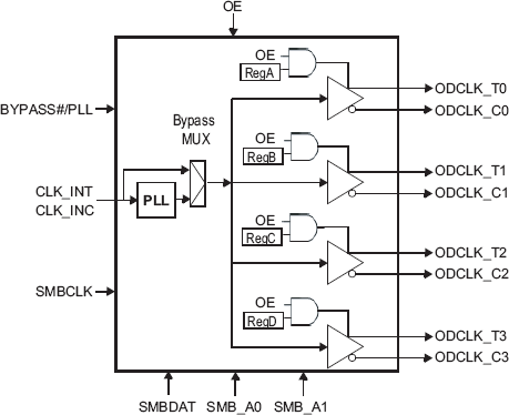
The 9214 clock generator provides the necessary clock signals to support the Rambus XDRTM memory subsystem and Redwood logic interface. The clock source is a reference clock that may or may not be modulated for spread spectrum. The 9214 provides 4 differential clock pairs in a space saving 28-pin TSSOP package and provides an off-the-shelf high-performance interface solution. Figure 1 shows the major components of the 9214 XDR Clock Generator. These include the a PLL, a Bypass Multiplexer and four differential output buffers. The outputs can be disabled by a logic low on the OE pin. An output is enabled by the combination of the OE pin being high, and 1 in its SMBus Output control register bit. The PLL receives a reference clock, CLK_INT/C and outputs a clock signal at a frequency equal to the input frequency times a multiplier. Table 2 shows the multipliers selectable via the SMBus interface. This clock signal is then fed to the differential output buffers to drive the enabled clocks. Disabled outputs are set to Hi-Z. The Bypass mode routes the input clock, CLK_INT/C, directly to the differential output buffers, bypassing the PLL. Up to four 9214 devices can be cascaded on the same SMBus. Table 3 shows the SMBus addressing and control for the four devices.