
| CAD Model: | View CAD Model |
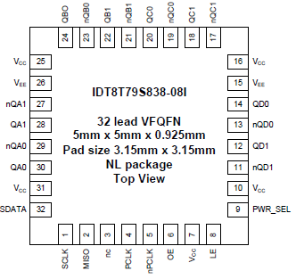
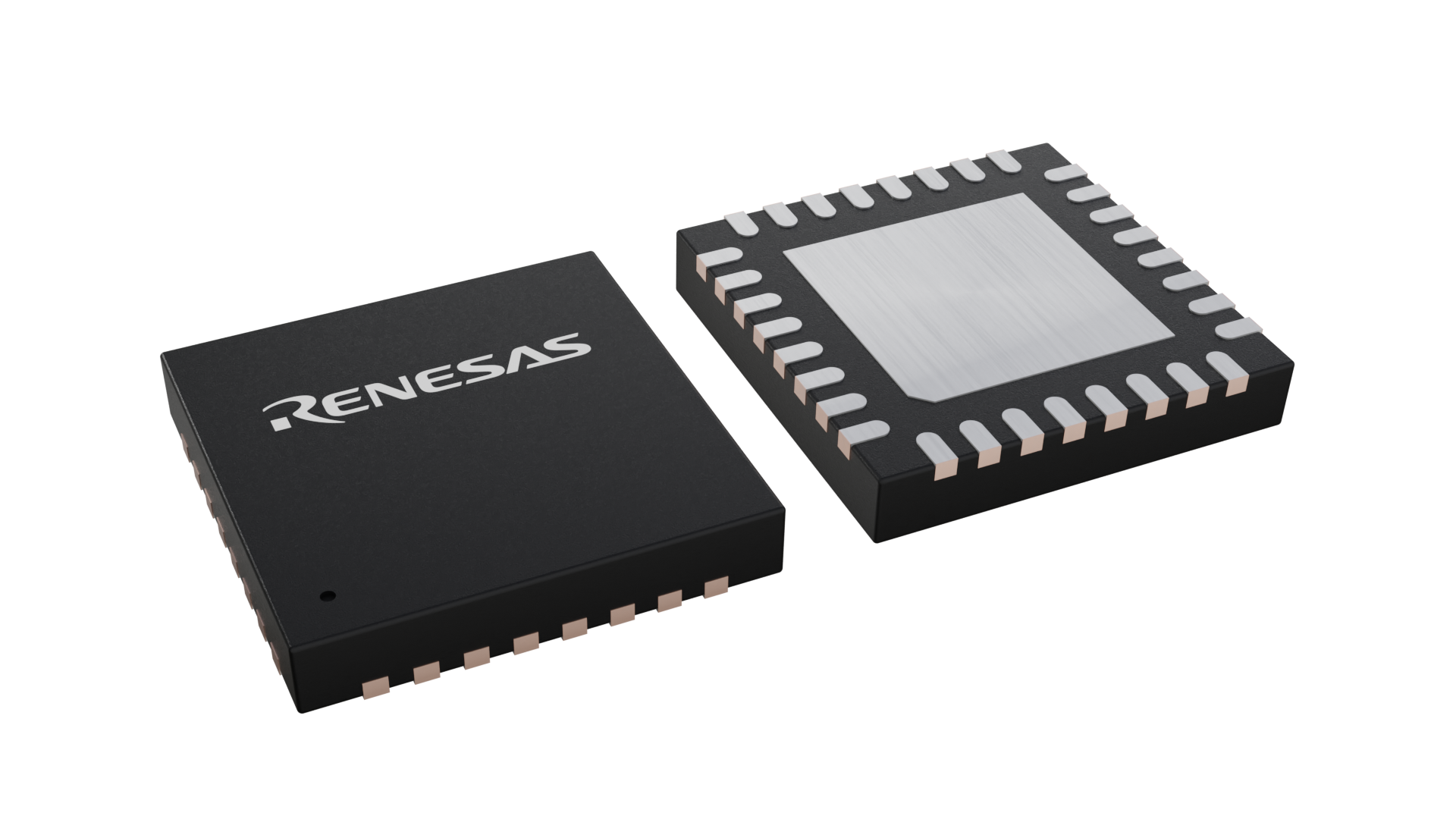
| Pkg. Type: | VFQFPN |
| Pkg. Code: | NLG32 |
| Lead Count (#): | 32 |
| Pkg. Dimensions (mm): | 5.0 x 5.0 x 0.9 |
| Pitch (mm): | 0.5 |
| Moisture Sensitivity Level (MSL) | 3 |
| Pb (Lead) Free | Yes |
| ECCN (US) | EAR99 |
| HTS (US) | 8542.39.0090 |
| Lead Count (#) | 32 |
| Carrier Type | Tray |
| Moisture Sensitivity Level (MSL) | 3 |
| Qty. per Reel (#) | 0 |
| Qty. per Carrier (#) | 490 |
| Pb (Lead) Free | Yes |
| Pb Free Category | e3 Sn |
| Temp. Range (°C) | -40 to 85°C |
| Core Voltage (V) | 3.3V, 2.5V |
| Function | Buffer |
| Input Freq (MHz) | 1500 |
| Input Type | LVPECL, LVDS |
| Inputs (#) | 1 |
| Length (mm) | 5 |
| MOQ | 490 |
| Output Banks (#) | 4 |
| Output Freq Range (MHz) | 1500 |
| Output Skew (ps) | 80 |
| Output Type | LVPECL, LVDS |
| Output Voltage (V) | 2.5V, 3.3V |
| Outputs (#) | 8 |
| Package Area (mm²) | 25 |
| Pitch (mm) | 0.5 |
| Pkg. Dimensions (mm) | 5.0 x 5.0 x 0.9 |
| Pkg. Type | VFQFPN |
| Product Category | Clock Buffers & Drivers |
| Requires Terms and Conditions | Does not require acceptance of Terms and Conditions |
| Tape & Reel | No |
| Thickness (mm) | 0.9 |
| Width (mm) | 5 |
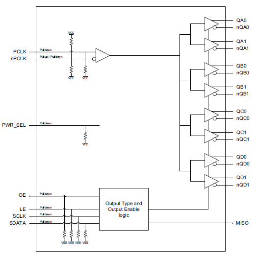
The IDT8T79S838-08I is a high performance, 1-to-8, differential input to universal output fanout buffer. The device is designed for signal fanout of high-frequency clock signals in applications requiring output frequencies generated simultaneously. The IDT8T79S838-08I is optimized for 3.3V and 2.5V supply voltages and a temperature range of -40°C to 85°C. The device is packaged in a space-saving 32 lead VFQFN package.