
Features
- One differential LVDS output pair and one differential feedback output pair
- One differential clock input pair
- CLK/nCLK can accept the following differential input levels: LVPECL, LVDS, LVHSTL, SSTL
- Input frequency range: 62.5MHz to 1GHz
- Output frequency range: 62.5MHz to 1GHz
- VCO range: 500MHz - 1GHz
- External feedback for "zero delay" clock regeneration with configurable frequencies
- Programmable dividers allow for the following output-to-input frequency ratios: 8:1, 4:1, 2:1, 1:1, 1:2, 1:4, 1:8
- Cycle-to-cycle jitter: 35ps (maximum)
- Static phase offset: ±100ps
- Full 3.3V supply mode
- -40°C to 85°C ambient operating temperature
- Available in lead free package

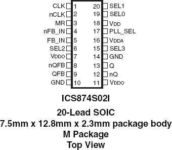
Description
The 874S02I is a highly versatile 1:1 Differential-to-LVDS Clock Generator and a member of the family of High Performance Clock Solutions from IDT. The 874S02I has a fully integrated PLL and can be configured as a zero delay buffer, multiplier or divider, and has an output frequency range of 62.5MHz to 1GHz. The reference divider, feedback divider and output divider are each programmable, thereby allowing for the following output-to-input frequency ratios: 8:1, 4:1, 2:1, 1:1, 1:2, 1:4, 1:8. The external feedback allows the device to achieve "zero delay" between the input clock and the output clocks. The PLL_SEL pin can be used to bypass the PLL for system test and debug purposes. In bypass mode, the reference clock is routed around the PLL and into the internal output dividers.